NE555->optocouler->Mosfet driving problems

Thread Starter

patpin

Joined Sep 15, 2012
401
Hello,
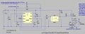
I try to simulate the driving of a transformer (ignition coil) with NE555 and an optocoupler. Anybody could tell me why the mosfet is not stopping to conduct when gate goes high? I see it remains at 26.5 A, which is probably why my secundary tension remains so low...
 

Attachments

Last edited:

Hypatia's Protege

Joined Mar 1, 2015
3,228
Looking at your shcematic, you have drain and source reversed. The body diode in the IRF5305 is conducting.
Indeed, the IRF5305 is a P-Channel device

@patpin
Further to post #2 --- If it was your intention to use an N-channel device -please be advised that a 10K pull-up isn't going to 'cut it' above a few tens of Hz... (to say nothing of 'ground reference' issues, etc...) -- Just reverse D & S in the circuit as shown and all should come well:)

Nice to see you on the fora again!:cool:

Best regards
HP:)
 
Last edited:

Thread Starter

patpin

Joined Sep 15, 2012
401
Indeed, the IRF5305 is a P-Channel device

@patpin
Further to post #2 --- If it was your intention to use an N-channel device -please be advised that a 10K pull-up isn't going to 'cut it' above a few tens of Hz... (to say nothing of 'ground reference' issues, etc...) -- Just reverse D & S in the circuit as shown and all should come well:)

Nice to see you on the fora again!:cool:

Best regards
HP:)
Hello, nice to see U active!!! I was aboad some time. (BTW the scope is OK)
I wanted a high side driver so thats why I took the P-chan. About the back EMf potentially destroying the optocoupler and furtther on. Do you think the zener at the primary is OK (as soon as connected)? Any other protection needed?
Why dont'I see the Voltage peaks (reverse) one normally see's (real life) at the primary?
 

Attachments

Hypatia's Protege

Joined Mar 1, 2015
3,228
About the back EMf potentially destroying the optocoupler and furtther on. Do you think the zener at the primary is OK
Firstly D3 is drawn 'backwards' (i.e. it would be under forward bias during MOSFET conduction).
Secondly the MBRS360 is a Schottky rectifier -- Not a Zener (granted - the symbols are similar:)).
Thirdly Q2 is at far greater jeopardy than U2 -- Still, it happens...:eek:

FWIW I would use a fast switching diode across the coil (cathode toward the drain of the mosfet) an MBR360 may well be 'up to the job' howbeit I'm dubious of its modest I{f} (3 Amperes) --- A good 'rule of thumb' RE: snubbers holds that peak 'kick' currents approach (but do not exceed) peak forward current through the inductor...

Why dont'I see the Voltage peaks (reverse) one normally see's (real life) at the primary?
I apologize that I'm less than useless with simulators!:oops::oops::oops:

Very best regards
HP:)
 

benta

Joined Dec 7, 2015
101
Question is, how you want to keep the primary voltage under control during turnoff to avoid damage to the MOSFET, and that in turn begs the question what you want your peak secondary voltage (spark) to be.

The Schottky that is shown on the schematic is the absolutely wrong choice.
My suggestion would be a bidirectional transorber across the primary, breakdown voltage around 18 V. You may need to help it a bit with a resistive/capacitive snubber in the same location.

Benta.
 

Hypatia's Protege

Joined Mar 1, 2015
3,228
My suggestion would be a bidirectional transorber across the primary, breakdown voltage around 18 V.
Assuming low frequency operation (i.e. ≤ 1kHz) I agree -- otherwise a gas discharge device or, better yet, a proper snubber network is the best approach...

Best regards
HP
 

Thread Starter

patpin

Joined Sep 15, 2012
401
Question is, how you want to keep the primary voltage under control during turnoff to avoid damage to the MOSFET, and that in turn begs the question what you want your peak secondary voltage (spark) to be.

The Schottky that is shown on the schematic is the absolutely wrong choice.
My suggestion would be a bidirectional transorber across the primary, breakdown voltage around 18 V. You may need to help it a bit with a resistive/capacitive snubber in the same location.

Benta.
20KV for secundary is OK; primary in function of that;
How do U dimension a snubbing network? I read that sometimes there are peaks of up to 400V on the primary (even if battery is 14,4V)
 

benta

Joined Dec 7, 2015
101
It would help a h*ll of a lot if you could describe what you are trying to do.
OK, spark ignition. Automotive?

What is the turns ratio of your ignition coil? You mention 20 kV secondary voltage, but that does not help us understand primary voltage.
Your traces suggest a switching frequency of around 100 Hz. But we don't know if it's higher or lower.

Dimensioning a snubber is not trivial. The parasitic inductances/capacitances of your coil are unknown, as well as the magnetic core properties and general circuit layout. The bidirectional transient absorber (eg, 1.5KE18C) is a start, but only when you have a prototype running, will you see the real spikes.
I'm a fan of simulators, but when working with magnetics, the end result always looks completely different to what they predict.

Benta.
 

Thread Starter

patpin

Joined Sep 15, 2012
401
Assuming low frequency operation (i.e. ≤ 1kHz) I agree -- otherwise a gas discharge device or, better yet, a proper snubber network is the best approach...

Best regards
HP
The Schottky that is shown on the schematic is the absolutely wrong choice.
My suggestion would be a bidirectional transorber across the primary, breakdown voltage around 18 V. You may need to help it a bit with a resistive/capacitive snubber in the same location.

Benta.
It would help a h*ll of a lot if you could describe what you are trying to do.
OK, spark ignition. Automotive?

What is the turns ratio of your ignition coil? You mention 20 kV secondary voltage, but that does not help us understand primary voltage.
Your traces suggest a switching frequency of around 100 Hz. But we don't know if it's higher or lower.

Dimensioning a snubber is not trivial. The parasitic inductances/capacitances of your coil are unknown, as well as the magnetic core properties and general circuit layout. The bidirectional transient absorber (eg, 1.5KE18C) is a start, but only when you have a prototype running, will you see the real spikes.
I'm a fan of simulators, but when working with magnetics, the end result always looks completely different to what they predict.

Benta.
 

Thread Starter

patpin

Joined Sep 15, 2012
401
Hello,
I m not planning to realise a circuit. It is purely theoretical, though with the purpose of beiing able to analyse the scope waveforms from an old Volkswagen with electronic ignition and injection.
As for the specifs of a typical coil: You find it below.
As TVS I thought putting one with a Vbr of 50V. Do you think that a TVS can absorb anough energy stored in a coil?
testbeeld.jpg
 

benta

Joined Dec 7, 2015
101
Now there's something to work with!
You have a primary/secondary ratio of 1:100
This means that the the secondary voltage induced to the primary will reach ~450 V (max.) at a 45 kV (max.) spark voltage
In your place, I'd forget the IRF5305 immediately!!!

The right power switch would probably be a 1 kV IGBT. In this case you'll need to choose between a low-side switch (=easy drive) or a high-side switch (=optical drive and gate-supply charge pump, alternatively transformer drive) design. High-voltage transistors or IGBTs are generally only available as NPN or N-channel.

Have Fun.

Benta.
 

Thread Starter

patpin

Joined Sep 15, 2012
401
Now there's something to work with!
You have a primary/secondary ratio of 1:100
This means that the the secondary voltage induced to the primary will reach ~450 V (max.) at a 45 kV (max.) spark voltage
In your place, I'd forget the IRF5305 immediately!!!

The right power switch would probably be a 1 kV IGBT. In this case you'll need to choose between a low-side switch (=easy drive) or a high-side switch (=optical drive and gate-supply charge pump, alternatively transformer drive) design. High-voltage transistors or IGBTs are generally only available as NPN or N-channel.

Have Fun.

Benta.
When I was 30 years younger I made a electronic ignition with a thyristor and it survived many years.... This was before IGBT's existed. There must be a workaround I presume.
 

benta

Joined Dec 7, 2015
101
"When I was 30 years younger I made a electronic ignition with a thyristor and it survived many years.... This was before IGBT's existed. There must be a workaround I presume."

Well, thyristors usually withstand at least 600 V. And an SCR ignition is a well-known circuit.
Your IRF5305 will take 55 V.
I only pointed out that your coil will deliver up to 450 V on the primary, so perhaps a higher voltage device would be right. Your choice...

Benta.
 
Last edited:

Hypatia's Protege

Joined Mar 1, 2015
3,228
When I was 30 years younger I made a electronic ignition with a thyristor and it survived many years.... This was before IGBT's existed. There must be a workaround I presume.
Of course -in theory - almost any device (within reason) may be used as the switch (i.e. without regard to maximum interelctrode EMF specification) use of a 'low voltage' device, however, will require more 'involved' snubber/ 'transformation network' design --- Unless 'exploration' of snubber topology is part of your study, you may save yourself much agro via employment of a device exhibiting a greater maximum V[dss] figure:) -- You may take my word for it that the greater saturated R[ds] exhibited by such devices will be of little consequence in your application:cool:

Please keep us posted:)

Best regards
HP:)
 
Last edited:

Thread Starter

patpin

Joined Sep 15, 2012
401
"When I was 30 years younger I made a electronic ignition with a thyristor and it survived many years.... This was before IGBT's existed. There must be a workaround I presume."

Well, thyristors usually withstand at least 600 V. And an SCR ignition is a well-known circuit.
Your IRF5305 will take 55 V.
I only pointed out that your coil will deliver up to 450 V on the primary, so perhaps a higher voltage device would be right. Your choice...

Benta.
Thanks, this helps me a bit more. Is there a way to simulate such events as the back EMF in LTSPICE?
 

Hypatia's Protege

Joined Mar 1, 2015
3,228
Hallo do U mean Vdss > 1000?
Sorry for the confusion!:oops: -- "+1000" was merely 'shorthand hyperbole' signifying that I agree with @benta 's statement...

Can you suggest a robust HV mosfet resisting the back EMF?
Please understand that good design will include a snubber (in any event), howbeit the criticality of such considerations is significantly 'eased' via selection of high (Max) Vds switch devices... -- For efficiency and reliability I suggest implementation of a non-dissipative snubber arrangement -- Granting that such elaboration is unnecessary for avocational applications...

But to answer your question::cool:
FWIW I use the IXFH20N100P in my X-Ray 'generator' designs (i.e. high power EHT PSUs) with good results -- Don't mind the ≈ 700mΩ (effective) saturated Rds;)
In many areas of power conversion I've 'moved on' to IGBT technology - Of course there are pros and cons either way...


Best regards and good luck
HP:)
 
Last edited:
Top