 Facebook
 Google
 GitHub
 Linkedin
Hello all,
Working daily to become a better board designer and I welcome any constructive feedback you have to offer. Please keep it helpful and informative. Please dumb it down for me if you can as I am a newbie however any help is greatly appreciated.
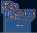
For this project which is a simple 7 segment counter using a 555 timer and 4026 IC chip I'm looking for feedback regarding my traces and routing. I deliberately chose a mix of THT and SMD components just to give myself a routing challenge. This was a project for learning and not construction so I can improve my routing skills.
please comment what i got right, wrong, needs improvement and why and if you have any other honorable mentions that come to mind the more the merrier.
for context:
thickest trace width near the 9V connector is 0.5mm
thinnest " " near the SW2 button is 0.25mm
Working daily to become a better board designer and I welcome any constructive feedback you have to offer. Please keep it helpful and informative. Please dumb it down for me if you can as I am a newbie however any help is greatly appreciated.
For this project which is a simple 7 segment counter using a 555 timer and 4026 IC chip I'm looking for feedback regarding my traces and routing. I deliberately chose a mix of THT and SMD components just to give myself a routing challenge. This was a project for learning and not construction so I can improve my routing skills.
please comment what i got right, wrong, needs improvement and why and if you have any other honorable mentions that come to mind the more the merrier.
for context:
thickest trace width near the 9V connector is 0.5mm
thinnest " " near the SW2 button is 0.25mm
Attachments
-
 113.9 KB Views: 25
")


