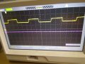
I asked for DC voltage measurements when the input is at 0VDC and at +5VDC. Instead you measured an AC squarewave without saying its extremely important frequency and duty-cycle.
I asked for DC voltage measurements when the input is at 0VDC and at +5VDC. Instead you measured an AC squarewave without saying its extremely important frequency and duty-cycle.
100kHz is too high for a circuit if it is built on a solderless breadboard that has a lot of stray capacitance between the rows of contacts and wires all over the place. Then the gates of the Mosfets get triangle waves so they spend a lot of time being linear and getting hot.
Wait a minute. With no load then the Mosfets are both conducting at the same time (current shoot-through) as they switch. They need a short pause so that one Mosfet turns off before the other Mosfet turns on.
You arrange for the switching waveforms to have no overlap. also called dead time. One classic way to do this is to derive the switching waveforms from a higher speed clock and a state machine.
If you want a 2 phase clock. You start with a clock and a state machine with 16 states. If you label the states 0 thru 15, then make the phase 1 clock low for states 8-15 and 0 and high for states 1-7. Then the phase 2 clock is low for states 0-8 and high for states 9-15. There is one clock tick of dead time between the two active states.
Q3 emitter voltage can only change by about 4V. Re-consider how you will use that to switch Q6 on and off reliably and whether a more conventional gate driving arrangement would be better.
long long time. hope you are well. 've designed the circuit, H-bridge with zeners. the waveform come all well at the four gates. One pmosfet on hgh side when soldered the waveform does not swing from 0-4 but from 2-4. The square wave starts from 2 to 4.It does not go to ground.... what could be the reason.
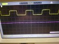
These are the waveforms observed at the gates of mosfet( without the mosfet soldered) . you can see the wave form at gate of n type mosfet, the waveform is perfect. at p type mosfet also its correct but after I solder the ptype mosfet the the waveform halves, causing the voltage not to rise to 27 V but remains at 22 volts. P channel mosfet thus remains on and heatts up.
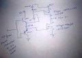
Your oscilloscope shows no extremely important voltage readings but the schematic shows what is wrong.
The gate voltage is much too low!
The IRF224 is so old it is not made by IR company anymore. It is rated at 250V(!) and has a poor on resistance when its gate voltage is at its rated 10V. Some of them barely turn on with your logic level gate voltage.
If your PWM source actually produces 5.0V pulses then the emitter-follower transistors produce gate voltages of only +4.7V for the N-Channel gate to turn on.
There is no datasheet for your P-channel IRF9224 which probably also needs a gate pulse voltage of 10V.
Look at a modern IRLZ44 N-channel Mosfet. Its maximum allowed load voltage is 55V and its on-resistance is 31 times or more lower than your old Mosfet when its gate turn-on voltage is only 4.5V. You can use a cheaper IRL540 that has a max load voltage of 100V and its on-resistance is 10 times lower than your old Mosfet when its gate turn-on voltage is 4.0V.
The L in the datasheet number means "logic level".
The P-fet never turns completely off. You need a level-shifter between the NPN emitter and the P-fet gate.
What is the intended purpose of the 1N4148? It just seems to confound the problem.
When you post schematics, use designators (R1, Q1 etc) for each component so that we can more easily discuss the circuit.
The 15V zener lifts the voltage to 27V. 1n4148 can be avoided I guess. The waveform distorts only when the mosfet is soldered. just before that the waveform at the gate is perfect. Could esd be a problem. i'll repost the schematic with designators tomorrow.
No.
The P-channel gate voltage is not driven to +27V which is higher than the 24V supply.
The NPN emitter-follower base might be driven as high as +5V then its emitter goes to +4.3V. Then the gate of the P-channel Mosfet goes to (15V + 4.3V=) +19.3V and is never turned off.
The output of the emitter-follower transistors go to +12V only if the base of the NPN goes to +12.7V.
But since the base goes only to 5V or less then the gate of the P-channel Mosfet goes to 4.3V+15V= 19.3V that does not turn off the P-channel Mosfet.
To fix that then you need a 20V zener diode but then when the PNP transistor gets 0V on its base, its emitter is +0.7V and the gate of the p-channel Mosfet will be +20.7V which is not low enough for it to turn on.
Therefore you need logic-level Mosfets or level shifters.
How will you increase the input from 5V to 12V?
Now the 15V zener has a voltage too high so the P-channel Mosfet is not fully turned on.
The 10k resistor feeding the high capacitance of the P-channel Mosfet gate turns it off VERY slowly. At any frequency it will never turn off.
How will you increase the input from 5V to 12V?
Now the 15V zener has a voltage too high so the P-channel Mosfet is not fully turned on.
The 10k resistor feeding the high capacitance of the P-channel Mosfet gate turns it off VERY slowly. At any frequency it will never turn off.
The Vgs threshold of a Mosfet is when it barely conducts only 0.25mA which is almost turned off. The low on-resistance is when Vgs is 10V.
The IRF9Z24 Mosfet is an ordinary Vgs=10V Mosfet, it is not "logic-level".
You need a logic level P-channel Mosfet, a 1K resistor and a lower frequency (20kHz?). Get rid of the useless diode.
 Facebook
 Google
 GitHub
 Linkedin