mosfet

Thread Starter

vultac

Joined Mar 2, 2009
142
no part number actually... just
"c2
88
v7"
along the body of the diode.....

Also isit possible to help me get an understanding of op-amp? Like the voltage supply... where in the datasheet can i see whats the max... and does the voltage supply (+V , -V) normally on top of and bottom of opamp in schematic.... determine how much voltage it can go?

and isit possible to say i want to limit my output voltage out from my opamp... isit possible to place the zener diode somewher along the opamp so it can limit it?

thanks!
 

Audioguru

Joined Dec 20, 2007
11,248
no part number actually... just
"c2
88
v7"
along the body of the diode.....
It might be an old BZX88c2V7 zener diode.

Also is it possible to help me get an understanding of op-amp? Like the voltage supply... where in the datasheet can i see whats the max?
The max ratings are near the front of the datasheet.

does the voltage supply (+V , -V) normally on top of and bottom of opamp in schematic.... determine how much voltage it can go?
The datasheet tells you how high and low the output goes with a certain supply voltage.

is it possible to say i want to limit my output voltage out from my opamp... isit possible to place the zener diode somewher along the opamp so it can limit it?
Usually the output voltage of an opamp is reduced with a zener diode across the feedback resistor.
 

Thread Starter

vultac

Joined Mar 2, 2009
142
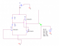
hi guys on this topic, GHAr post #62, i bleieved it was a totem pole connection? can someone expplain to me how the circuit works? and how the resistors can limit the voltage? because when i try playing with R2 values... i can actually limit my voltage meaning if i put in 16V into it it will give 16V and 8V... and if R2 were different value it will give 16V ~5V mebe? :confused:
 

Attachments

Thread Starter

vultac

Joined Mar 2, 2009
142
Another thing is guys.., for PMOS right..

Vs = 17V... to on i need 5V~7V ya? but how come when i simulate the program using a pulse of 17V high and 0V low it still works just that the voltage ripple is less for the output...

it seems like offing it is only important... meaning if it were 15V source... and if gate can produce 15V it works.... but seems like its not dependant on the on voltage? i used +15V and +0V for this it still works... where the theoretical shud be +15 and 5V? cos vgs (on) = -10V?

did for the others as well like 13V 12V etc... same thing... just that voltage output ripple is less..
 

Audioguru

Joined Dec 20, 2007
11,248
thx audio guru... im looking at this LM358AN datasheet.... http://www.national.com/profile/snip.cgi/openDS=LM358

can u point out where the parameters i need to see is at?

my input is a 0V~ 5V and i want the output to be 20V.. DC... isit possible to achieve it using that op amp? and the supply rial.. i dont really understand wad does it do lol
The LM358 dual and the LM324 quad opamps are the slowest opamps ever made. They have trouble at frequencies over only 2kHz.

Instead, use one of the many opamps that also work with a single supply, that have inputs that work at ground and have an output that goes to ground like an MC34071 single, MC34072 dual or MC34074 quad.
 

Wendy

Joined Mar 24, 2008
23,801
That isn't quite a totem pole, it is a dual emitter follower. It is a bit mushy, but if you try to move 0.6V (base emitter) outside it's middle it firms up. It is capable of some decent currents, which makes it good for output drivers for op amps, at least in digital mode. Between the two base emitter junctions you have an indeterminate zone of around 1.4 V, where neither transistor Q3 or Q1 is turned fully on. This range sounds wide, but remember it is actually ±0.6V. If you try to use it in a linear mode it will usually create crossover distortion.

Boosting weak devices

Another scheme I've been using looks like this...


It inverts, and it can have good drive, but if you try for too much from the transistors it will wimp out. BTW, the transistor configuration on the 555 is a good example of a totem pole output. TTL logic uses something very similar.
 

Wendy

Joined Mar 24, 2008
23,801
The LM358 dual and the LM324 quad opamps are the slowest opamps ever made. They have trouble at frequencies over only 2kHz.

Instead, use one of the many opamps that also work with a single supply, that have inputs that work at ground and have an output that goes to ground like an MC34071 single, MC34072 dual or MC34074 quad.
I just shared some samples with Wookie, NJM4565. For a 35¢ part its not bad. It is not low voltage however, nor does it go to ground on the input well (I think). 4Mhz freq response and 6V/µs slew rate. I think it has a ±5V minimum power supply spec.

I'll have to get some of those parts you suggested for myself.

Wookie had an interesting design for a MOSFET driver for a LED buck boost circuit.

http://forum.allaboutcircuits.com/showpost.php?p=266376&postcount=20

If you look close it is also a dual emitter follower. I'm going to try using the central theme of the design form my ideas.
 

Attachments

Last edited:

Audioguru

Joined Dec 20, 2007
11,248
hi guys on this topic, GHAr post #62, i bleieved it was a totem pole connection? can someone expplain to me how the circuit works?
The output transistors are complementary emitter followers. they can supply a fairly high current to quickly charge and discharge the high gate capacitance of a Mosfet.

The two resistors are a voltage divider when Q2 is turned on so they produce a certan voltage.
For example with the 16V supply and the 1k and 250 ohm resistors, the voltage at the junction of the resistors is +16V when Q2 is turned off. Then the output of the emitter followers is 16V - 0.7V= 15.3V.
When Q2 is turned on then the voltage at the junction of the resistors is [16V/(1k + 250 ohms)] x 250 ohms= 3.2V. The output of the emitter followers is 3.2V -0.7V= =2.5V or 3.2V + 0.7V= 3.9V.

The Vgs of most Mosfets is 10V for them to turn on very well. But if you make the Vgs 12V, 15V or 18V then they turn on better. The max allowed Vgs is 20V.
 

Thread Starter

vultac

Joined Mar 2, 2009
142
bill/audio :

thanks,... but im still unclear about the different type of common emitter....well in short can i just say that... that circuity i posted #120 the supply acts as a source to boost any input to that voltage level? because ive tried an input pulse of +5V and +0V into it it boost up to 16-0.7 around +15.3V ~ 0V? somewhere around there? but i realized that the input to that circuit if i dont put a nand gate its very noisy... when i put a nand gate it becomes smoother any explanation? im going to post the output graph...

audio:

thanks, but can u give me more detail like how the current flow... throw which switch more thorough? hshaha... sorry ya i need to really understand then i can aply... and for the mosfet i assume for the one u said abt Vgs 12v etc ur talking about a NMOS? for me i used pmos so i guess its the opposite ya? i.e Vs = 15V, to get a good turn on my Vg can range from -20V~+5V? yea? becauyse for pmos its Vgs -10?
 

Thread Starter

vultac

Joined Mar 2, 2009
142
so basically on my post #120 Q2 is the input ya and the output is the one connected to nothing...

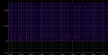
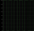
here are the graphs

first picture_54, blue is my input used (+5V , +0V) and the red is the output of nand gate think around (860mV +0V)

and picture 55, output... smooth nice square wave. with nand gate that is


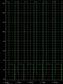
Without the nand gate,
Using same input (+5,0V) i get a weird noisy curve as shown on picture_56...any explanations y?
 

Attachments

Audioguru

Joined Dec 20, 2007
11,248
Ordinary Mosfets need a Vgs of 10V to turn on fully. Of course the polarity must be with a gate that is more negative than the source for a P-channel, and a gate that is more positive than the source for an N-channel.

Since the max allowed Vgs is 20V then 12V, 15V or 18V can be used.
 

Thread Starter

vultac

Joined Mar 2, 2009
142
ok... thanks for the info... mosfet and all is so hard to understand hahahahaha... i don think i can ever understand if i were to read it by myself :/

heres the nand gate..
 

Attachments

Put a resistor between the NAND gate and Q2 or else it shorts into the base. That overdrive could have been your noise source and all the NAND gate is doing is reducing the current compared to what the signal generator was providing.

Put a resistor between the collector output of Q2 and base of Q3 or else they are a short from ground to V+ through the base diode junction of Q3.

To reduce shoot through, stack diodes one either side of your input to the bridge transistors. Actually shoot through is not such a big problem because you are not in an H-bridge.

I would have suggested an H-bridge instead of a follower bridge. You can invert your signal again maybe with a spare from your NAND gate IC, in order to allow you to swap position of Q1 and Q3. Common Emitter instead of Common Collector should give you better drive with less time in the active phase for your Mosfet. You could also use a noninverting predrive in place of Q2.
 

Audioguru

Joined Dec 20, 2007
11,248
Your extremely old TTL "NAND gate" is wired as a simple logic inverter. A transistor can do the same thing.
When the input goes high then the output goes low at up to 16mA.
When the input goes low then the output goes high at a low current.
 

Thread Starter

vultac

Joined Mar 2, 2009
142
potato/audio..

realized that when i tested it this morning, the output signal is very "noisy" when i increased the voltage of the source to the transistors... yah im using common emitter config just that i rotated Q3... also the resistor from the nand to Q2.. wad value shud it be? and how do i calculate it? :(

so the nand gate just force it to low current? anything to do with the circuit pulling up the signal or something?
 
Last edited:

kingdano

Joined Apr 14, 2010
377
i think you need to start poking/prodding the circuit with an oscilloscope and trying to understand how its working without looking at the details so much.

right now (IMO) you need basic behavioral understanding of the circuits blocks.
 
I sort of steered you wrong.

Don't bother with going to an Hbridge because it won't make enough good differences for you to notice, but without adding some complications and components you are likely to have latching, shootthrough, and other problems. So forget switching them to Common Emitter. I thought about explaining how to do it and then realized it is not worth it. It was not that good an idea.

With 16V, common collectors in a follower bridge will get it done if it can be done at all.

You need resistors between a base and the input signal. How big a resistor is not as important as having a resistor. So between 2k2 and 68k and experiment to see what works.

You just need something to limit current (a base driven by 10milliamps with 100 gain would allow 1 Amp of current which is more than you need).

The resistors cover the voltage between the base and the input level is another way to look at it.
 
Top