MOSFET fail short - searching for cause

Thread Starter

Marcel DaJanchar

Joined Sep 9, 2015
32
Hello everyone!

I have stumbled upon a mysterious problem regarding my circuit. The output MOSFETs are getting shorted due to unknown reason (at least to me).

Circuit function:
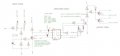
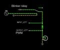
My circuit is a simple 555 PWM generator with external trigger on the RESET pin. PWM is enabled until one (or both) external triggers are pulled high. Then the PWM is disabled for several seconds (depending on RC part). When no trigger is applied, PWM is enabled again. Output of the 555 is wired on two MOSFETs, which drives cars blinkers (lamps 21w). The problem is, that my circuit was working good (no overheating and fully functional) for about a month. Few days ago the output of one MOSFET shorted to VCC causing only one blinker to stay on (this short was holding gate of other MOSFET on VCC). Am I missing some gate protection on MOSFET where spike can occur and damage it? PCB is safely placed in a box (so no shorts to GND can occur).

More details:
External triggers are INPUT_LEFT and INPUT_RIGHT
VCC is car battery voltage (12V-15V, depending whether car is running or not)
ZENER_VCC is refering to 5V, generated on seperated circuit
Output MOSFETs are Q3 and Q5. Both are P-channel MOS AO3401 (http://www.aosmd.com/pdfs/datasheet/AO3401.pdf)
D3 is zener diode (10V)
T2 is 2N3904

Sorry for my english, as it is not my first language. Also this is my first post.
Thanks for all the answers
 

Attachments

dl324

Joined Mar 30, 2015
16,937
Welcome to AAC!

Relevant portion of the schematic:
upload_2019-1-1_9-28-22.png
Is the load on the MOSFETs inductive?

Your schematic style is difficult to read. If you print the schematic, all of the text origin marks won't be shown. That would help a little.
 

Thread Starter

Marcel DaJanchar

Joined Sep 9, 2015
32
Sorry for messy picture. I have attached PDF version of this circuit. Hope it helps.

Load is one light bulb (12v 21w) per MOSFET, so the load is mostly ohmic. This two bulbs are blinkers. I was suspecting the blinker relay coil but this two bulbs are wired on the load side of relay so there is no connection with the relay's coil, I suppose.
 

Attachments

wayneh

Joined Sep 9, 2010
17,498
What is the purpose of R4? I can't see how it does anything useful. Not a problem, just no purpose.

I'm wondering about the situation when/if a bulb disconnects or fails open. Does that present a risk to the MOSFET since the drain pin is no longer grounded?
 

Thread Starter

Marcel DaJanchar

Joined Sep 9, 2015
32
@wayneh You are right, the R4 serves no purpose there. It was already omitted in my design (forgot to delete it in schematics).
Also nice theory on floating drain. One more question on this theory: Is there any chance that output MOSFET could fail if VCC is disconnected? I have VCC wired on car battery through a switch. The VCC is floating when the switch is turned off, right?

@LesJones As you see in my first post, the output MOSFETs are AO3401 (P-channel MOS). I just used BSS84 in my schematics because of a symbol.

Thanks
 

dl324

Joined Mar 30, 2015
16,937
Sorry for messy picture. I have attached PDF version of this circuit. Hope it helps.
It's an improvement. Next time, print in black and white. Color coded schematics are distracting if the color isn't significant. Differentiating between text, components, and wires isn't significant...
Load is one light bulb (12v 21w) per MOSFET, so the load is mostly ohmic. This two bulbs are blinkers. I was suspecting the blinker relay coil but this two bulbs are wired on the load side of relay so there is no connection with the relay's coil, I suppose.
Are you saying that the loads are bulbs? Or are the loads relay coils that switch the bulbs?
 

twohats

Joined Oct 28, 2015
447
"This two bulbs are blinkers. I was suspecting the blinker relay coil but this two bulbs are wired on the load side of relay so there is no connection with the relay's coil, I suppose. "
Can we rule out a relay coil?
Marcel, can you include the relay and bulbs, in your schematic?
Regards, Two hats...
 

dl324

Joined Mar 30, 2015
16,937
That would be hard to say, because I noticed that problem when I got out of a car (hard to see front blinkers when driving :) )
If you can determine that they don't fail when the car isn't running, that would eliminate voltage spikes from the charging system as a problem.
 

dl324

Joined Mar 30, 2015
16,937
I'll take notes about making schematics more easy to read.
I never did like the timer symbol in Eagle, it never lent itself to good flow. It was almost as bad as using pin order. I modified it in my version of Eagle.

With this redraw, I think circuit intent more apparent; even without the labels in your schematic.
upload_2019-1-1_15-29-53.png
You have some inputs controlling an oscillator that drives the output.

R4 is unnecessary, D3 might be. Can't tell if the input to Q4 makes sense without knowing more about the inputs.
 

Thread Starter

Marcel DaJanchar

Joined Sep 9, 2015
32
@dl324 wow, many thanks for this! I agree with R4 being unnecessary. My first design had D3 as gate protection diode. When I realised that FETs are already opened at Vgs being 4.5V or more for needed current of 2A, I added resistor divider (R3 and R8). Car battery voltage is always around 12v (lets say 10-16V), so voltage at gate pin will be around 5-8V. Do you think I should remove D3? Can resistor divider prevent spikes on gate pin as D3 would, or should I use both (divider and protection zener diode)?

As for the input:
D1 and D2 are there to prevent reverse current flow from capacitor C1.
R1 is there to limit current for charging capacitor C1.
R12 and C1 are main components or RC delay for putting 555 in reset (delay is around 1s).
R10 and R2 are wired as resistor divider for signal FET there (Q4).

I have added R13 because without it, the voltage never reached 0V on C1 (was always around 0.7 - 1V at C1). Unfortunately I have no explanation why.
 

dl324

Joined Mar 30, 2015
16,937
Do you think I should remove D3? Can resistor divider prevent spikes on gate pin as D3 would, or should I use both (divider and protection zener diode)?
The zener will only afford protection if the charging system voltage is above 20V. There can be spikes as high as 80V, so it might still be needed.

While I was searching for a datasheet for the MOSFET you're using, some eBay listings showed up for about a nickel each. That was too good to be true, so I checked a few of the listings. They were all for counterfeit parts.

Manufacturers don't have such messy markings:
upload_2019-1-1_17-44-16.png
upload_2019-1-1_17-44-57.png

I can't tell if these are counterfeit, but they also have a different marking:
upload_2019-1-1_17-45-51.png

Counterfeit parts could be the cause of your failures. Can you post a close up, clearly focused picture?
 

dl324

Joined Mar 30, 2015
16,937
As for the input:
D1 and D2 are there to prevent reverse current flow from capacitor C1.
R1 is there to limit current for charging capacitor C1.
R12 and C1 are main components or RC delay for putting 555 in reset (delay is around 1s).
R10 and R2 are wired as resistor divider for signal FET there (Q4).

I have added R13 because without it, the voltage never reached 0V on C1 (was always around 0.7 - 1V at C1). Unfortunately I have no explanation why.
Then I'd draw the input this way:
upload_2019-1-1_19-11-21.png
R12 isn't necessary, you can adjust R1 and/or R13 if removing R12 changes charging/discharging time significantly.
 

Thread Starter

Marcel DaJanchar

Joined Sep 9, 2015
32
Here, I have made some photos of these MOSFETs.
On the first photo, the FET is marked with red circle. On the second image you see the FET which failed. As the image quality is not significant, I can tell that both of the FETs are marked with A19T on it. FETs were bought on eBay yes.
 

Attachments

Top