MC14538B as astable ?

GopherT

Joined Nov 23, 2012
8,009
View attachment 110282 Oh, wait. Where can I get a low impedance output? Need a buffer?

View attachment 110281
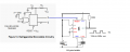
No, Q and /Q in the bottom circuit are complementary outputs. You need to bring the signal from the top (astable) circuit into the "B" I out in the bottom monostable. Monostable triggers on falling edge.

Then you can take an output of the bottom into a mosfet's gate. Source to ground and drain to your device (then to positive supply). Select Q or not-Q as output to drive mosfet gate depending on duty cycle needed. At 350Hz, I think you can drive logic level directly - even with a 4538.
 

Thread Starter

inwo

Joined Nov 7, 2013
2,419
My output comes from the top astable. As complimentary outputs are both used, I need a buffer on one of them.

Any additional components are a deal breaker as far as simplest circuit.
It's hard to beat this............555 makes a good output device.
I'll pick a mono. with schmitt input.
 

Attachments

Alec_t

Joined Sep 17, 2013
14,328
If you want to use the monostable to gate the astable, then connect the B input of the astable to the appropriate Q or -Q output (not sure how you want to gate it) of the monostable instead of to Vdd (9V) as shown.
The 100k loads (90uA if Vdd=9V) on the astable outputs are trivial. A buffer would only be needed if you wanted to draw more than 2 mA or so.
 

AnalogKid

Joined Aug 1, 2013
11,055
Concept-only at this point. No clue how to simulate this, but it looks like it should work. It might require an input duty cycle less than 50%. Maybe move the retrig network after U1B, and put an edge extractor after U1A. Hmmm...

With the input held high, adjust R2 for 350 Hz output. With the input at 350 Hz squarewave, adjust R1 for steady-state high at U1 pin 4.

ak
Osc-Gate-1-c.gif
 

Attachments

Last edited:

Thread Starter

inwo

Joined Nov 7, 2013
2,419
Thank you, that fits the KISS request.
Often I don't explain things well. Jumping between projects, it may be a while before testing it.
 

Thread Starter

inwo

Joined Nov 7, 2013
2,419
Good news have some 4093s. :)

Gated oscillator works with .1 and 33k it's in ballpark.
Only getting a low level sawtooth from first stage so far.
 

AnalogKid

Joined Aug 1, 2013
11,055
The R3-C3 differentiator probably will work better with another 1N914 (or 4148) diode in parallel with R3, cathode to Vcc, anode to pin 5.

ak
 

Thread Starter

inwo

Joined Nov 7, 2013
2,419
Caught up enough to get back at this.

Nothing worked so I went back to my original circuit using a 74123 gating a 555 timer.
That seems to work fine.

Switching the 74123 to a 14538 will not work.

I believe my problem is "why does the 74123 work at all?"

My whole theory seems to be wrong. Yet it works.
 

Alec_t

Joined Sep 17, 2013
14,328
All unused inputs of any CMOS circuit should be tied high or low as appropriate.

Edit: Reference to Reset removed.
 
Last edited:

AnalogKid

Joined Aug 1, 2013
11,055
For the *unused* half, ground all inputs except R/C. You don't need a capacitor there, but I'd tie it to Vcc with a resistor just in case its input wants a little current limiting.

ak
 

Thread Starter

inwo

Joined Nov 7, 2013
2,419
cd14538.gif
12 low
11 high
13 low
14 pull up
15 low

Or can I tie them all low?
 
Last edited:

Thread Starter

inwo

Joined Nov 7, 2013
2,419
Think I see how it works now.
Thought he gate pulse from monostable could allow. multiple astable pulses.

Now I see, that when adjusted properly, both are near the same rc.

Output is one pulse per input, until retriggering enables 555 continuous on.

Right now I'm not seeing problems.

Will try to build one solid enough to test in actual tach circuit.
 

Thread Starter

inwo

Joined Nov 7, 2013
2,419
Sorry about deletions.
Didn't want anyone wasting there time on a simple error.
I was getting spike on the gate connection between monostable and 555.
The bad thing was, or good, the circuit worked fine.
You know how you get in the habit of tying pin 4 and 8 together on 555s?
Well, it made me forget which was which.
P4 and P8 mixed up in diagram and pcb.
So I was gating by powering 555. Doh!

So don't do this...........................post 32
MVC-017F.JPG
 
Top