Facebook
 Google
 GitHub
 Linkedin
Hi,
An initially charged capacitor in a resonance circuit undergoes periodic voltage reversal (blue line), as shown below:

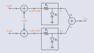
A possible circuit to address this problem uses 2 capacitor banks & switch modules, as shown:

C₁ and C₂ represent metallized film capacitor banks of equal capacitance, but the main difference is that the voltage across C₁ will always be ≥0 (0⇔+10 kV) whereas the voltage across C₂ will always be <0.
In order to achieve a sinusoidal decay current waveform, switches SCR₁ through SCR₄ will have to be switched on (via microcontrollers V₁ through V₄) in a particular sequence, according to the following conditions:
· SCR₁: IF (V(C₁)>0 && V(C₂)==0,V₁=4,V₁=1)
· SCR₂: IF (V(C₁)==0 && V(Lᴄᴏɪʟ)<0,V₂=4,V₂=1)
· SCR₃: IF (V(C₁)==0 && V(C₂)<0,V₃=4,V₃=1)
· SCR₄: IF (V(C₁)==0 && V(Lᴄᴏɪʟ)>0,V₄=4,V₄=1)
Basically, here is a quick explanation:
1. upon closing of SCR₁, C₁ discharges until V(C₁)=0
2. SCR₁ turns off and SCR₂ turns on so that current flows through C₂; V(C₂)<0 (e.g. –9.95 kV) when fully charged
3. SCR₂ turns off and SCR₃ turns on
4. C₂ starts discharging through SCR₃ until V(C₃)=0
5. SCR₃ turns off and SCR₄ turns on
6. C₁ is charged by the inductor until V(C₁)≈10 kV (slightly less than +9.95 kV due to circuit resistance)
7. cycle repeats itself
Here is a screenshot of the schematic showing the SPICE directives and comments:

A copy of the schematic is attached below. I would like to verify that the above hypothesis is correct and to derive a current waveform through each capacitor bank.
I ran into trouble trying to implement the boolean logic into this schematic, and I would greatly appreciate it anyone who could help with this.
Thanks!
An initially charged capacitor in a resonance circuit undergoes periodic voltage reversal (blue line), as shown below:
A possible circuit to address this problem uses 2 capacitor banks & switch modules, as shown:
C₁ and C₂ represent metallized film capacitor banks of equal capacitance, but the main difference is that the voltage across C₁ will always be ≥0 (0⇔+10 kV) whereas the voltage across C₂ will always be <0.
In order to achieve a sinusoidal decay current waveform, switches SCR₁ through SCR₄ will have to be switched on (via microcontrollers V₁ through V₄) in a particular sequence, according to the following conditions:
· SCR₁: IF (V(C₁)>0 && V(C₂)==0,V₁=4,V₁=1)
· SCR₂: IF (V(C₁)==0 && V(Lᴄᴏɪʟ)<0,V₂=4,V₂=1)
· SCR₃: IF (V(C₁)==0 && V(C₂)<0,V₃=4,V₃=1)
· SCR₄: IF (V(C₁)==0 && V(Lᴄᴏɪʟ)>0,V₄=4,V₄=1)
Basically, here is a quick explanation:
1. upon closing of SCR₁, C₁ discharges until V(C₁)=0
2. SCR₁ turns off and SCR₂ turns on so that current flows through C₂; V(C₂)<0 (e.g. –9.95 kV) when fully charged
3. SCR₂ turns off and SCR₃ turns on
4. C₂ starts discharging through SCR₃ until V(C₃)=0
5. SCR₃ turns off and SCR₄ turns on
6. C₁ is charged by the inductor until V(C₁)≈10 kV (slightly less than +9.95 kV due to circuit resistance)
7. cycle repeats itself
Here is a screenshot of the schematic showing the SPICE directives and comments:
A copy of the schematic is attached below. I would like to verify that the above hypothesis is correct and to derive a current waveform through each capacitor bank.
I ran into trouble trying to implement the boolean logic into this schematic, and I would greatly appreciate it anyone who could help with this.
Thanks!
Attachments
-
7.5 KB Views: 9
Last edited: