OK<
So, its maybe its not connected correctly in the circuit or it a fake.
Remove the 2N3055 and check that you have the Base and Emitter correctly identified and wired.
E
OK<
So, its maybe its not connected correctly in the circuit or it a fake.
Remove the 2N3055 and check that you have the Base and Emitter correctly identified and wired.
E
Eric, i measure the voltage from the INPUT, it is 26v with no load, but when i put Load, the voltage of input dropout is only 20v. Is that my source can not supply my needed current ? because i only use full bridge with 2A diode?
Hi,
I would say as the 2N3055 is not getting warm and the BD139 is overheating, there is a problem with the 2N3055 transistor or its connections.
E
Use your Ohm meter and check the 2N3055 as the image shows, post what you measure.
Why does it look like you are changing feedback factor to regulator,
rather than using reference and the pot into error amp ? That
compromises regulation.
Not a 723 expert but seems like the wrong way to implement the adjustment
point. In the datasheet it shows pot connected to Vref and NI input right
way to do adjustment.
hi absf,
The TS states that the BD139 is getting hot and the 2N3055 is not getting warm, I agree the 2N3055 is not passing any current.
I have asked him to to check the wiring.
E
Nope. Visualize the error amplifier as an ordinary op amp summing circuit with multiple signals applied via individual resistors to the summing node. The gain for each input is independent of the gain for any other input, each individually determined by the ratio of the feedback resistor to the input resistor. In this case there are two inputs and the non-inverting input is at a fixed (reference) voltage. That means that R2 has a fixed voltage across it (Vref), so it drops out of the equation. It doesn't seem intuitive, but if you do the arithmetic that is how it behaves.
As is typical in power supply design, the error amplifier runs open-loop at DC and the frequency compensation components, in this case just a cap, set the AC gain, which is of course frequency dependent. It is much easier to analyze for the matter at hand if you use a fixed feedback resistance.
I agree that adjusting the reference is often much superior. A lot of the power supply work I did required adjustability over a wide range, so I used the fixed-divider (might differ from model to model of the supply), variable-reference method. Varying the reference voltage is a whole lot easier than varying the divider ratio when you want to do it with a processor or remotely. If you fiddle with the feedback you've got risk of noise and disaster if the path is broken. You can only fiddle the resistor from the inverting input to ground or you change the frequency response unless it is "flat." That makes the range limited and non-linear. If you fiddle with the reference, you can filter it to next to zero bandwidth for many applications and if the path goes open, the output goes to zero - unless you really botch your design. With switcher control ICs, using the adjustable reference method usually requires some treachery and deceit to get around the fact that there is almost always an internal reference to the non-inverting input of an internal error amp. Plus I often had to have three control loops (this for CP - constant voltage, constant current and constant potential, where each established a limit with "automatic crossover.") I miss doing power supply design - much the same way I miss having cornflakes in my bed when they aren't there anymore.
Boy I am having a problem seeing this. The NI input is connected to Vref thru R3, for bias
offset ? Or to decouple the NI input from Vref ? So R1 and R2 form a divider feeding back a
fractional part of Vout to inverting input, thereby effecting the control loop. If Vout rises, the
R1/R2 junction rise, the Amp gains that up in a negative direction, dropping
base drive for output transistor, and lowering the V. Am I losing my marbles ?
As you say the loop keeps servoing the junction of R1/R2 to equal Vref, but the
correction loop is the divide change in Vout reflected back to the base drive,
after being gained up and inverted, by the amp.
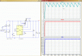
Reading thru this thread (especially "ebp" post #36), and reading the datasheet, I came up with this:
Minimum voltage can be adjusted by changing the value of R3.
The graph show the output pot adjusted in 10% steps.
thnks all u for trying help me so much, finally i found exactly the problem. It is not my transis at all, that is LM723, my boss is disappointed with me, and he told that i must to do it, with all cost. He told that i need to buy for him more 2 LM723 and i did it. I use the new lm723 and it operated properly. I check it again, with Load up to 3A, output only drop 2v, and 2n3055 heat quickly. But the fake is not, it drop as half, and 2n3055 is cold like winter. The fake chip drove me into a corner, i am so dissappointed with myself that i can not complete a simple schematic
 Facebook
 Google
 GitHub
 Linkedin