Latch circuit designing.

Thread Starter

Isidoro Ibañez Labiano

Joined Nov 4, 2016
28
Thank you all, for your time and support.

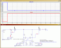
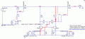
So far, I will go for the last circuit within my design, and I will test it (hardware).
I will let you know the outcomes/results and any modification that could come into my mind.

Thanks again!
 

ericgibbs

Joined Jan 29, 2010
21,442
hi,
I cannot explain that difference.?
This my plot using your asc file.

Have you changed any of the settings in the tools options.??
 

Attachments

ericgibbs

Joined Jan 29, 2010
21,442
hi,
That plot you posted is due the setting in .tran 'starting the sim at 0V.

The voltage offset of Vout now has suddenly appeared!!

There is small current flowing via R3,R2,R12 and Q2 Base > Emitter, this means that Vgate is below the VBAT and so theM1 FET is slightly ON.[conducting]

E
 

Thread Starter

Isidoro Ibañez Labiano

Joined Nov 4, 2016
28
hi,
You could consider this option.
E
Thank you very much for your time @ericgibbs!

I have refined the circuit (attached).
I would like to use it for both 8V and ~17V. And I have built a prototype and it works, but the consumption it's a bit high ~3mA (at 8V).

I have thought to change R1 and R2 for 10K, that is fine. But if I change R3 and R4 as well, then for 8V it is fine and for 16.8V I have a residual Vout (~2.70V).
Could you explain me why? Could I fix it?

Thanks again for your time in advance.

Warm regards,
Isidoro
 

Attachments

Thread Starter

Isidoro Ibañez Labiano

Joined Nov 4, 2016
28
Hi Eric,

Thanks again for your reply and for your time!
The problem with the solution that you have proposed me, is that then I cannot control the output with SET and RESET.
I could not see that Voltage spike when I measured my prototype.
Now I would like to know why there is that spike in my simulations. So, more the theoretical aspect than an actual solution.

Cheers,
Isi
 

ericgibbs

Joined Jan 29, 2010
21,442
hi,
I see that you are using BJT's in place of the FET's for the bistable.
The BJT circuit now has a 2V Gate to Source voltage on the output MOSFET during the Off period, so there is an Output voltage.

I will look see what can be done.

E
 

ericgibbs

Joined Jan 29, 2010
21,442
hi,
The FDS4465 has a Vgate threshold of ~ 1v, which means when using BJT's for the bistable, the Vgate is greater than 1.5v, so the FET never switches Off.

Is there a reason you decided to use BJT's in place of the FET's.

E
 

Attachments

Thread Starter

Isidoro Ibañez Labiano

Joined Nov 4, 2016
28
Hi,

There is not a specific rationale behind that choose.
Those 2N2222s are very robust for ESD and also radiation, I like that. But, my main concern is about current consumption.
I need to check how to reduce the current consumption, any advice for achieving that goal?

Thanks!

BR,
Isi
 

ericgibbs

Joined Jan 29, 2010
21,442
hi,
I would have thought ESD and radiation would not be a problem for a FET bistable.?
Is the circuit working in an hazardous, electrically noisy environment.
E
 

Thread Starter

Isidoro Ibañez Labiano

Joined Nov 4, 2016
28
Hi,
Yes, it is.
But current consumption is critical, as well. Indeed that is more important.
I am checking more latching circuits to have more options, and for consuming less current. Any suggestion from your side (@eric)?
Thanks!
Cheers,
Isi
 

ericgibbs

Joined Jan 29, 2010
21,442
hi,
For lowest current consumption FET's are the best solution.
Once the bistable FET's are wired into the circuit I would not expect ESD to be a problem.
Also the circuit already has two MOSFET devices.

I suppose the unit is going to be electrically shielded.?

E

EDIT:
Could you say how this project is going to be used.??
 
Last edited:

Thread Starter

Isidoro Ibañez Labiano

Joined Nov 4, 2016
28
Hi Eric,

Yes, the unit is going to be electrically shielded (it will be handle with ESD precautions as well).
This latch circuit is for a power system, for switching it ON.

Thanks again for your support! Much appreciated.

Cheers,
Isi
 
Top