Is this pcb layout going to short anywhere?

Thread Starter

Bod

Joined Sep 18, 2016
317
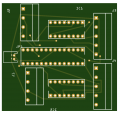
I have created a pcb schematic and have routed it. It would be nice to know if this would short anywhere or whether it would actually work. This is one of the first boards I have ever made so forgive the messiness of it. I have tried to keep it as small as I can. Here are some images of it.

Schematic:
Screen Shot 2018-07-30 at 11.19.12.png

PCB layout:
Screen Shot 2018-07-30 at 11.25.12.png
Please ignore the missing link on the connector over on the right. That was meant to join to ground.

Thanks in advance,
Bod.
 

Thread Starter

Bod

Joined Sep 18, 2016
317
Ignore that design, I just remade it here is the (better) one:
Top:
Screen Shot 2018-07-30 at 13.56.47.png
Bottom:
Screen Shot 2018-07-30 at 13.56.56.png
EDIT: I got the PCB wrong again since I put in the wrong dimensions in the PCB viewer. This caused components to be cut off at the top and bottom. With the new pictures it looks like there are more problems on the right problems.
 

Attachments

Last edited:

jpanhalt

Joined Jan 18, 2008
11,087
Did you run a DRC? Some of those clearances, including the one circled in red, look a bit small. You can go around the left end of that device and avoid that problem.
 

Thread Starter

Bod

Joined Sep 18, 2016
317
Did you run a DRC? Some of those clearances, including the one circled in red, look a bit small. You can go around the left end of that device and avoid that problem.
I used Fritzing to make this layout. I also used auto-routing. Is a DRC possible in Fritzing?

EDIT: The pictures of the pcb where taken from the gerber viewer in JLCPCB.
EDIT 2: I have just done a DRC and fixed some of the overlapping traces. There are still a few I don't know how to get rid of. The image is of the problematic areas.
Screen Shot 2018-07-30 at 14.13.21.png
Thanks,
Bod.
 
Last edited:

jpanhalt

Joined Jan 18, 2008
11,087
Suggestions:
1) DRC as you found out is a design rules check. You can change the rules, but generally, things like changing a clearance from the default might be a bad idea for DIY boards. For commercially made boards, the board house will have set its limits. In fact, some places have their DRC files that you can down load and use in your program (e.g., Oshpark provides its design rules files for EAGLE).

2) I am a little familiar with Fitzing, but not to the level to know what tools it offers. Many of us here, myself included, will not download an unfamiliar program just to view an image or file. Please post snippets or typical images (e.g., PNG, JPG, GIF or PDF). I find pdf useful as I just set my printer to print to pdf , copy, and paste.

3) Since this thread is about finding problems in your board design, when you change that design please post a new response with the changed design. Please do not edit a previously posted image, as that makes it much more difficult for those less familiar with your design to track the changes.

4) Electronically, having traces and branches at all sorts of odd angles is probably not a problem, but it loses some of the aesthetic appeal of a board laid out with 90° and 45° angles (and their complements), except where it might be necessary to deviate from that. Some people object strenuously to having 90° bends. I don't. You will even find such examples from major manufacturers. Another advantage of using those standard angles is that tracks lay nicely parallel to each other, so an overlay of two tracts on the same side is very obvious.

Let's restart with an image (color if possible) of each side of your board as you currently have it. At this point, posting the transparency showing both side is probably not helpful.
 

Thread Starter

Bod

Joined Sep 18, 2016
317
Thank for the reply. As for number 2, that's fair enough; I thought someone might have Fritzing so they could have a look at it. Number 3, I only did so becuase I didn't want to spam posts.

So far, here is the top:
Screen Shot 2018-07-30 at 15.33.12.png
And here is the bottom:
Screen Shot 2018-07-30 at 15.33.18.png

There is only one main problem with two bottom layer traces overlapping. The neatness of my traces aren't really an issue for me because only I am going to see it.

Thanks,
Bod
 

mcgyvr

Joined Oct 15, 2009
5,394
An autorouter produced that crap?
yuck..
What clearances are you trying to use?
Many of those traces look too close to other nets..
Many seem to be less than trace width in spots..

I want to suggest you ditch that Fritz junk if thats the output after DRC/Autorouting.....
 

Thread Starter

Bod

Joined Sep 18, 2016
317
Some of the autorouting was ok. A lot of what is messy was me moving traces so they didn't touch other pads or traces (I am using default clearance). I used Eagle for my first pcb but I found it quite confusing. Ill try Eagle again.

Thanks,
Bod
 

MrChips

Joined Oct 2, 2009
34,855
PCB layout is called "artwork".
Notice the word "art". In other words, a PCB layout should be a piece of art that you would be proud of creating.

Here are some tips:
  • Keep your lines straight, horizontally and vertically.
  • Avoid corners at right-angles. Make 45° bends at the corners.
  • Keep clear of pads and vias. Take advantage of the space when you have it.
  • In general, the shortest trace between two nodes is the best solution.
  • When creating a double-sided PCB, routing becomes easier if you maintain horizontal lines on one side and vertical lines on the other.
 

mcgyvr

Joined Oct 15, 2009
5,394
Ill try Eagle again.

Thanks,
Bod
I would not suggest trying Eagle again..
I would suggest trying Diptrace.. You will likely find Diptrace to be hands down better than Eagle.. Install it and follow the tutorial from start to finish and you should be up/running in no time..
I use it professionally and find it quite capable and quite easy/logical in its use..
I tried Eagle and ran into the same confusion as you..
 

Thread Starter

Bod

Joined Sep 18, 2016
317
I have tried Diptrace and I definately like it, and will use it. But since I couldn't be bothered to redo my circuit again I tried Eagle out and for some reason, it just clicked and now I don't find eagle that confusing.

Anyway, thank you for all the help about the best way to layout a pcb. I will make sure to take this into consideration!

Thanks,
Bod.
 
Top