Is this a Class C amplifier?

BR-549

Joined Sep 22, 2013
4,928
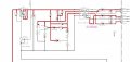
OK...use your scope just like a DDM. Reference to ground and look at EVERYTHING in the circuit.

You might need to make amplitude and centering adjustments for different parts of the circuit. If the display looks solid or fuzzy......decrease time base.

Now connect the second channel (referenced to ground).......and watch different parts of the circuit at the same time that you are watching channel 1. Notice the difference?

For instance......adjust channel 2 at the top of R3752, for centered bottom half of scope screen and then look at all the other parts of circuit with channel 1 centered in top half of scope screen.

Now repeat for the base of the transistor as a reference.

I assume you have compared audio channels before. This frequency will be higher....you will have to decrease time base.
And the amplitudes will be different.

Can you make any sense of what you see? Can you apply the basics?

Can you see why it's called a switch?
 

BR-549

Joined Sep 22, 2013
4,928
JMono.......hold on a second.....your missing the big picture. Please refer to the print in post #10. To understand this circuit, you need to understand how transformer T3702 works. This whole circuit is to control the flux in T3720.

This is not used as a normal transformer. T3720 supplies a controlled flux to the two/three rectifier circuits.

This is where the basics come in. Do you know what the magnetizing effect to a core is?

In this application.....we do not want it. This is what the network....D3752, C3752 and R3756 does.

Most would say that this network is a snubber....to protect the transistor. But in this case the network de-magnetizes the core. It resets the core flux. This allows the fine flux control required. The saturation curve always goes thru zero.

Do you recall magnetizing flux curves? Did anything I said make any sense?

Do you understand what feedback is?
 

Thread Starter

JMono

Joined Mar 5, 2017
19
BR-549, I do understand feedback, not the magnetizing effect of a core, was never covered. Your insight is very much appreciated. I am looking for an overview of how this circuit is functioning. My schooling was 30 years ago. What started this search was curiosity. I happened to be checking the voltages on the PCB this circuit was on, noticed 5.6V as the supply voltage, assumed the transistor base voltage would be .6V referenced to ground. It however was the -.4V I stated earlier.
 

Jony130

Joined Feb 17, 2009
5,488
Here you have a simplified schematic

RCC_01.png

As you can see we have a transformer with three windings. The primary winding Np, secondary winding NS. And one additional auxiliary winding Na.
And notice the "DOT" notation on the diagram. https://en.wikipedia.org/wiki/Polarity_(mutual_inductance)#Terminal_layout_conventions
Na - positive feedback winding.
R1 - starting resistor.
C1 together with D3, D4 form a "peak detector" to give us information about the output voltage (Ns winding) and C1 is charged via D3 D4 when Q1 is OFF. The secondary winding Ns voltage (output voltage) is "reflected" as a Na voltage. And this voltage is then rectified via D3, D4 diode and smoothed by C1 capacitor. The large the output voltage the large is the voltage across C1 capacitor (more negative voltage). However, D1 Zener diode becomes conductive to cut the base current of Q1 transistor, thereby speeding up the turning OFF for Q1. So, D1 and C1 voltage will regulate the output voltage. Lower Vout --->lower VC1 voltage, therefore Q1 will be Turn-ON for the longer time before D1 diode cut the base current. And longer T_ON time means that we have store more energy in the core. So we can transfer more energy into the load (more energy = increases in output voltage).

And here you have the transformer voltage polarities when Q1 is TURN-ON. And "positive feedback" current. Note than D6, D5 and D3,D4 are OFF

RCC_02.png

And when Q1 is Cut-OFF
RCC_03.png
This time D3,D4 diode are ON and D5, D6 are also ON.

Once again I encourage you to read this
http://mmcircuit.com/understand-rcc-smps/
http://www.dos4ever.com/flyback/flyback.html

assumed the transistor base voltage would be .6V referenced to ground. It however was the -.4V I stated earlier.
You are reading the negative voltage because DC voltmeter will "show" you the average value.
 

BR-549

Joined Sep 22, 2013
4,928
The base voltage should be referenced to the emitter........not to ground.

30 years is too long. You have a meter and a scope........get a breadboard and some parts.

This circuit would be hard to breadboard....but only because of the transformer. There are many oscillator and switching circuits you can build and study.

Not to mention what these new microprocessors and IC chips can do.

And you have all the collective knowledge of mankind at hand.
 

Thread Starter

JMono

Joined Mar 5, 2017
19
BR-549, for myself , I don't want to get bogged down in theory. I don't have the training to look that deeply into it. I am trying to grasp the over all functions of the components, and then understand the complete circuit. The flux is the thing? On a side note, is this the Kornfield Kounty BR-549?
 

Thread Starter

JMono

Joined Mar 5, 2017
19
Jony, the voltage at C3752 ( C1 in the example you have given), is -5V. At which point does the Zener conduct to turn the transistor off?
 

Jony130

Joined Feb 17, 2009
5,488
so to be clear here, C3751-D3751-R3756 have no affect on the transistor switching?
http://blog.fairchildsemi.com/2014/...e-rcd-snubber-flyback-converter/#.WMwF52emk2w

Jony, the voltage at C3752 ( C1 in the example you have given), is -5V. At which point does the Zener conduct to turn the transistor off?
Let me try to explain this to you despite the fact that I'm not SMPS specialist.
Frist, you have to remember that when Q1 is ON (in saturation) almost all supply voltage is applied across the primary winding (Np).
This means, that the current in the primary inductor start to ramp up in rate equal to ΔI/Δt = V/L (the rate of current change (dI/dt) in amps per second)
Where L is the primary winding inductance and V is the voltage across it.
The base current is mainly provided by auxiliary winding and by R2, D2. So, as Ic current increase (ramp up) Vbe voltage also increses.
Now let me assume that the C1 capacitor was previously charged (when Q1 was OFF) to -5V with respect to ground (Output voltage increase). And the Zener diode breakdown voltage is 5.6V.
At the beginning of a cycle when Q1 turns ON the diode D1 diode is at the edge of conduction.
But as current in the primary winding inductance increases the Q1 Vbe voltage also increases, which turns-ON the Zener diode more. And the Zener diode starts to steal the current from the Q1 base.

RCC_0.4.png

This will cause the Q1 will start to come out of the saturation region, thereby speeding up the turning OFF for Q1. Therefore we store less energy in the primary winding inductance and Vout will be reduced. We have some kind of negative-feedback mechanism. When the voltage at the output drops the C1 capacitor voltage will also be reduced. For example to -4.9V. So the Zener diode will now start conducting the current if the Q1 Vbe voltage is larger than 0.7V, therefore primary winding inductance current can reach higher value (store more energy). And more energy means increase in the output voltage.
In real life, the situation is much more complicated because, for example, the Zener diode "knee" is not sharp enough. And this is why the voltage regulation is very bad. And I'm sure that the Yamaha engineers add additional linear LDO voltage regulator after this DC/DC converter.
 
Last edited:
Top