I will need help about a TTL and signal double design

Thread Starter

hsui

Joined Dec 5, 2021
5
Hello everyone
I am trying to finish a circuit that about to reversal and boost the signal. The signal is a +3.3V as input and I wound the output between 9V to around 0V (bigger than 0V but smaller than 1V).As the blow fig show. That is the signal I want.3.PNG
I was looking at the MAX913 and their level shift circuit. However, I cannot finish and simulate what I want. If you have any idea about that, please let me know.
More details. I have a signal as this2.PNG
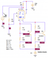
This is my input signal. And circuit I have now is
1.PNGP.S. on MAX web
I wish the circuit can be as basic as possible. I mean if you can only use RLC and Dio that will be great.
Please let me know if you have any idea and any source about that.
 
Last edited by a moderator:

ronsimpson

Joined Oct 7, 2019
3,037
Run the MAX from a 10V to 0V supply. (could be 12V supply)
Set R1, R2 to 3.3/2=1.65 volts. (switch in the middle of 0V and 3.3V) (or choose the voltage at any point you want)
The outputs should output 0 or 10V.
1638753052680.png
 

ronsimpson

Joined Oct 7, 2019
3,037
The antique TTL IC has such a low output voltage and current that your circuit will not work.
That circuit (in the data sheet) is used to level shift the outputs. There are several examples of moving the output voltages up or down 5 volts. It does not do what he wants. (even if it works)
 

Thread Starter

hsui

Joined Dec 5, 2021
5
R1 = 33K
R2 = 10K
Thank you for the info. I tried something close to your values and your values as well. The output is kind of ok, but not very well. The attached screenshot shows that the output has a dot on the top. This is why I used TTL at the beginning. Please let me know if you have any idea how to remove that.
1644516969338.png
 

AnalogKid

Joined Aug 1, 2013
11,037
What is the image in post #9? What does each color represent? Why do both signals go all the way down to 0.000 V? A real transistor cannot do that, and most simulation programs also know that.

There are no reactive components in the circuit, and the circuit has no feedback path. Without either of those, that spike is very difficult to make happen. It probably is a simulation artifact. IOW, it probably will not be there in real life with real components.

What is the circuit for? More directly, what does the output of this circuit connect to? The signal at an open-collector output is affected by whatever the output is connected to and driving.

ak
 
Last edited:

sghioto

Joined Dec 31, 2017
5,388
lease let me know if you have any idea how to remove that.
I agree with ak it's probably an artifact from the simulator. Can't you breadboard that simple circuit for your own satisfaction?
It's important to know what the output is connected to because it could involve a complete re-design.
 

Thread Starter

hsui

Joined Dec 5, 2021
5
I agree with ak it's probably an artifact from the simulator. Can't you breadboard that simple circuit for your own satisfaction?
It's important to know what the output is connected to because it could involve a complete re-design.
Agree, and thank you for the help. The result is from the simulation. The thing is I am waiting for the lab to give me really circuit resolt. All I can say at this point is I am trying to use a circuit and convert a signal upside down. So, the circuit converts a signal and sends it to the control unit. Thanks for help ak, sghioto, and everyone.
 
Top