Facebook
 Google
 GitHub
 Linkedin
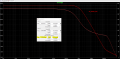
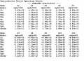
A gain-bandwidth product of 5GHz? That's pretty tall order. In Texas Instruments' entire portfolio they only have four that can exceed that. It's not the sort of thing you could knock together out of a handful of mediocre small power MOSFETs.I would like to make a device that respects the typical performance of a multistage amplifier (amplification of a small differential signal, a gain of around 80/100dB, a bandwidth in the order of tens of KHz, phase margin respected...)
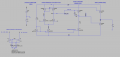
I have a problem to implement a common source Cascode gain stage in the multistage amplifier design
- Thread starter PorzDesign
- Start date