Help with switching a negative supply (Mosfet switch for a negative supply)

Thread Starter

k2n2a2

Joined Jul 16, 2012
37
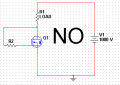
There is really something wrong in the way you look at MOSFET switches. First of all if you connect a resistor from gate to source , it is not floating. Having a floating gate means it is not connected to anything.

The basics is really simple:
Apply a positive voltage from gate to source within the Vgs limits and it will conduct.
Apply 0V (low impedance source, not floating) or a negative voltage from gate to source and it will cease to conduct. Unless you apply a voltage to the source that is more positive than the drain voltage in which case it will conduct through the body diode.

How you denominate your 1000V voltage in your circuit doesn't matter, what I just said holds true. (n-channel MOSFET)
thanks for clearing that up for me, I didnt fully understand the concept of floating gate. youre right, the gate is connected to the drain with a resistor, so that I guess doesn't make it floating..

you know, the thing that messed me up is how make the gate of that mosfet:
1- either connected to ground (so it conducts),
2- or just have it pulled down by the gate-source resistor, without connecting it to ground or VCC or anything other than the gate-source resistor (so it doesn't conduct).
If I can achieve that, my problem is solved.

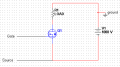
I was thinkig of using a relay to control that gate, either connect it to ground or just no contact with ground or anything except the gate-source resistor (what I used to call "floating")...
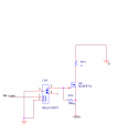
image 4.png

this way the PWM will control whether the mosfet gate is only connected to the RGS resistor (which pulls the gate voltage down to -1000 to make the fet turn off) or either connect the gate to ground (which then makes the transistor conduct).

it is just that I have never seen any mosfet being driven this way before.
what do you think?
 

praondevou

Joined Jul 9, 2011
2,942
youre right, the gate is connected to the drain with a resistor, so that I guess doesn't make it floating..
I didn't say that.
connecting the gate to drain when the voltage at the drain is 1000V is not a good idea. You are lucky you didn't blow it up.


you know, the thing that messed me up is how make the gate of that mosfet:
1- either connected to ground (so it conducts),
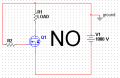
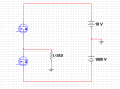
You don't want it connect to ground if your "ground" is the positive of the -1000V power supply. Like here:

This will immediatly destroy your MOSFET.

2- or just have it pulled down by the gate-source resistor, without connecting it to ground or VCC or anything other than the gate-source resistor (so it doesn't conduct).
If I can achieve that, my problem is solved.
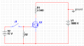
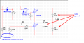
You mean like this:

Not impossible but as you can see there is another power supply involved. The voltage at the gate changes now from -1000V to -985V with respect to ground. Or from 0V to 15V with respect to the source terminal.
At 100kHz you do not want to discharge through a resistor (which has to be bigger than a few ohms in order to limit current). This will take too long and you will increase switching losses.

I was thinkig of using a relay to control that gate, either connect it to ground or just no contact with ground or anything except the gate-source resistor (what I used to call "floating")...
Do not use a relay. The contacts bounce.

You said the PWM source is galvanically isolated from the -1000V. So just connect the PWM's ground to -1000V and the PWM signal via a gate resistor to the MOSFETs gate.

Look at the following picture: The only thing you need to know is that the voltage from gate to source should NEVER exceed the ratings in the datasheet. That's depending on the MOSFET from +-10V to +-30V.
 

Attachments

Thread Starter

k2n2a2

Joined Jul 16, 2012
37
If I leave the PWM isolated (not connect its ground to the power ground) would that work?
would would be the gate voltage (coming from the PWM source) be in refrence to?
what I am saying is, dont we need a closed loop from the gate to ground?


I will try that anyway and post the results.

Thanks
 

praondevou

Joined Jul 9, 2011
2,942
If I leave the PWM isolated (not connect its ground to the power ground) would that work?
would would be the gate voltage (coming from the PWM source) be in refrence to?
what I am saying is, dont we need a closed loop from the gate to ground?


I will try that anyway and post the results.

Thanks
Yes you need a closed loop. From the PWM signal to the gate and from the source back to the reference voltage of the PWM signal.

If you use the term "ground" please always mention what "ground" you are referring to. The power ground of the -1000V is connected to the load which is connected to the drain of the MOSFET. In the above circuits you will never connect the PWM reference to this "ground" but to the source of the MOSFET.
 

Thread Starter

k2n2a2

Joined Jul 16, 2012
37
I was the told the duty cycle is about 20% most of the time, but it could vary.
This circuit that you posted a few days ago is very good actually. in fact I came up with something very similar to that (low side and high side driver).-1000V.PNG

can you show me how to drive both transistors, given one PWM signal?

--I already figured out how to drive the high side switch (the positive supply switch)--
 

praondevou

Joined Jul 9, 2011
2,942
This circuit that you posted a few days ago is very good actually. in fact I came up with something very similar to that (low side and high side driver).View attachment 44874

can you show me how to drive both transistors, given one PWM signal?

--I already figured out how to drive the high side switch (the positive supply switch)--
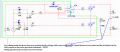
My assumption: The PWM reference is separated from the rest!


Please read carefully:

1. I used -100V for the simulation instead of -1000V. Doesn't matter.
2. C1 charges to 15V when Q1 is closed. That means the duty cycle must be such that C1 can fully charge before it's being transfered to the gate of Q2.
3. Replace U1 with an isolated gate driver like the one I posted somewhere before, something like the HCPL3180 for example. Don't use R4. I forgot the gate resistor for Q2.
4. You must add something to create a deadtime. Tell us if you need assistance.
5. The two major power supplies and the load have the same reference now. The PWM does not. Isolation between PWM circuit and the rest should be more than 1500V.
 

Attachments

Thread Starter

k2n2a2

Joined Jul 16, 2012
37
Thanks a lot for clearing that up for me. That's exactly what I was trying to get at..
What is the deadtime creator part that you used here?
Is it and inverting gate with 2ns delay?
And also, the pwm ground is connected to the source of the bottom transistor (Q1) which means its connected to the -100V, is that safe?
 

praondevou

Joined Jul 9, 2011
2,942
Thanks a lot for clearing that up for me. That's exactly what I was trying to get at..
What is the deadtime creator part that you used here?
Is it and inverting gate with 2ns delay?
And also, the pwm ground is connected to the source of the bottom transistor (Q1) which means its connected to the -100V, is that safe?
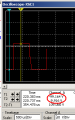
1. the deadtime is created by the RCD combination before the CMOS schmitt-trigger gates. It delays the turn-ON of the MOSFETs. It's around 2micro seconds here.
2. If it's safe depends on your circuit. If for example someone will be able to touch ground AND anything in the PWM circuit it will NOT be safe.


.......................
And we didn't even talk about the problems you may run in to switching 1000V at 2A, i.e. layout considerations...

EDIT: you need also a gate driver for the lower MOSFET to provide a good amount of current when charging/discharging the gate. It doesn't need to be isolated though.
 

Attachments

Last edited:

Thread Starter

k2n2a2

Joined Jul 16, 2012
37
Thank you for explaining that..

the PWM that controls the switching is 100KHz with 20% duty cycle, which means my period is 10us. therefore my pulse train is: 2us is high(to switch the positive supply on for 2us), and the next 8us the PWM is low (to switch the negative supply on).
where would the dead time fit in this picture?
and is there alternative for the dead time? specially that I am not supposed to mess around with the pulse width and period?
I am aware that we have to make sure that the two mosfets should NEVER be on at the same time (otherwise it will be disaster), which is why you are suggesting adding the dead time here. I was going to accomplish this by making the two switches identical (same mosfets, same drivers, etc) to make sure they both have the same propagation delay and the same rise/fall time to prevent both mosfets from being on at the same time.
any thoughts?

And I really appreciate all your feedback and help.
 

praondevou

Joined Jul 9, 2011
2,942
Thank you for explaining that..

the PWM that controls the switching is 100KHz with 20% duty cycle, which means my period is 10us. therefore my pulse train is: 2us is high(to switch the positive supply on for 2us), and the next 8us the PWM is low (to switch the negative supply on).
where would the dead time fit in this picture?
It doesn't. 2us was just an example.

I am aware that we have to make sure that the two mosfets should NEVER be on at the same time (otherwise it will be disaster), which is why you are suggesting adding the dead time here. I was going to accomplish this by making the two switches identical (same mosfets, same drivers, etc) to make sure they both have the same propagation delay and the same rise/fall time to prevent both mosfets from being on at the same time.
Yes, this what you have to make sure. I wouldn't rely on only the turn-on, turn-off times of drivers and MOSFETs. Give them at least a few 100ns safety margin.

And once you start your test I recommend doing it with a lower voltage.

BTW, this is all theory. I never build something like this switching 1000V at 100kHz. You may run into unforeseen difficulties when actually building it.
 
I have a question about the way this circuit works:
if the current from the 1000V supply flows to the drain of Q3 (which is connected to the plus side of the power supply) , then the current will exit the source of Q3 and try to enter the source of Q2.
Would that work (current entering the Mosfet from the source)?
Unless you meant that Q2 is PMOS (but the symbol is for NMOS), if Q2 in NMOS VDS will be negative.
Shouldn't the two MOSFETs be in series?
Thank you.
Yes it works, but it depend about how are you driven the mosfet, I am working with 800vcd power supply, but if you can show an images, would be better to help you
 
Top