Help with Circuit Design - Signal Isolation

Thread Starter

mriksman

Joined Aug 31, 2010
113
Can I summarise , see if I have this right.

The FL5150 is expecting a 0 to X linear analog control voltage, and the opto-isolators are as you have seen not linear and not repeatable across temperature and different devices. ( diode forward current /light is none linear , transistor is none linear )

I see you have tried PWM , but that as you have seen , this needs power.
I have two ways to approach this;
  1. get the PWM digital signal over the optoisolator to the FL5150 side. Linearity of the optoisolator doesn't matter then. However, choice of load resistor does - it effects switching speed - distorting the PWM signal.
  2. filter the PWM signal on the controller side, and use the optoisolator to send the analog signal across. This has the benefit of not requiring Vdd from FL5150 at all, but as you say - issues with optoisolator linearity. I can get around this; either use a $3 linear optoisolator, or use a dual optoisolator and assume both are reasonable similar (see previous schematic). But it assumes the FL5150 having 10uA at the DIM Control Pin for EVERY FL5150 I buy - however, the datasheet says it can range from 7-13uA. Which means big differences to the voltage it would see when using a 250k resistor (1.75V for 7uA, 2.5V for 10uA, etc...)

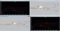
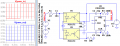
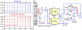
PWM is fine, as it is powered by a separate 3.3V supply for the controller. However, the optoisolator collector pin is connected to the Vdd (5V) of the FL5150 (as it is the only positive '..supply' on that side). It appears trying to source more than 3mA from that Vdd pin, the FL5150 crashes. So I am limited to using a load resistor of around 4.7k. This causes the PWM signal to get distorted, affecting the voltages at lower dimming levels (see below - see the separation between the lower lines are larger than the higher lines)

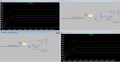
At the moment, I think I will use the following (maybe with/without the op-amp; I still need to test actual results. It seems to give better results);
1591100539667.png
 

Attachments

Deleted member 115935

Joined Dec 31, 1969
0
Why did you settle on the FL5150 ?
not certain what I can do for you here, I'm not certain is this for a on off / home use , or a commercial product and what your level of experience is. These voltages can be deadly, at one time talking about mains voltage stuff was banned on forums.


There are plenty of computer controlled ways to dim mains lamps,
e.g. https://www.instructables.com/id/Arduino-controlled-light-dimmer-The-circuit/
This case, the arduino is just providing the PWM signals which you already have.

The orriginal lamp dimmers is this sort of thing,

https://www.watelectrical.com/light... circuit of light,charge from the main supply.

this goes back to far for me to remeber, but is a good set of notes

https://www.epanorama.net/documents/lights/lightdimmer.html
 

Alec_t

Joined Sep 17, 2013
15,156
Be great to have a good model for it, but so far my practical tests aren't giving me promising results.
I've debugged the H11LxM models and their symbols. They're in the attached zip file.
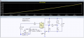
Although the models could be made to go down to 0V output, I've modelled the minimum as ~90mV, I don't know what the real-world opto output can go down to. It depends on the saturation voltage of the output transistor. To get lower voltage you might be able to use the opto output to drive a push-pull pair of logic-level MOSFETS.

IsolatedPWM.png

Edit:
Reducing R2 and R3 (e.g.to 270R and 330R, respectively) improves the linearity of the curves shown, but you may need then to increase R4 to keep the Dim control happy. However, those lower resistance values mean more current draw from Vdd, so it looks like that would be an issue if 3mA is the max practical value :(.
 

Attachments

Last edited:

Alec_t

Joined Sep 17, 2013
15,156
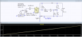
Add a CMOS gate to the mix and you get low current draw, Dim_ctrl voltage down to virtually zero** and excellent linearity :

IsolatedPWM2.png

** Edit:
I've just re-read the datasheet for the FL IC.
Taking Dim-ctrl down to 0V switches the IC into low power mode. Presumably that needs the power re-cycled to bring it back to normal mode.
 
Last edited:

Thread Starter

mriksman

Joined Aug 31, 2010
113
Why did you settle on the FL5150 ?
not certain what I can do for you here, I'm not certain is this for a on off / home use , or a commercial product and what your level of experience is. These voltages can be deadly, at one time talking about mains voltage stuff was banned on forums.


There are plenty of computer controlled ways to dim mains lamps,
e.g. https://www.instructables.com/id/Arduino-controlled-light-dimmer-The-circuit/
This case, the arduino is just providing the PWM signals which you already have.

The orriginal lamp dimmers is this sort of thing,

https://www.watelectrical.com/light-dimmer-circuit-using-triac/#:~:text=The basic circuit of light,charge from the main supply.

this goes back to far for me to remeber, but is a good set of notes

https://www.epanorama.net/documents/lights/lightdimmer.html
FL5150 supports both leading and trailing edge. Most dimming circuits use a TRIAC; which generally have poor compatibility with AC LED lights. This $1 FL5150 handles zero crossing, over current protection, and the choice between leading and trailing edge, and keeps components count down. It’s an obvious choice.

Thanks for the interest, but I am almost done thanks to the great input from @Alec_t and @crutschow.
 

Thread Starter

mriksman

Joined Aug 31, 2010
113
I've debugged the H11LxM models and their symbols. They're in the attached zip file.
Although the models could be made to go down to 0V output, I've modelled the minimum as ~90mV, I don't know what the real-world opto output can go down to. It depends on the saturation voltage of the output transistor. To get lower voltage you might be able to use the opto output to drive a push-pull pair of logic-level MOSFETS.

View attachment 208744

Edit:
Reducing R2 and R3 (e.g.to 270R and 330R, respectively) improves the linearity of the curves shown, but you may need then to increase R4 to keep the Dim control happy. However, those lower resistance values mean more current draw from Vdd, so it looks like that would be an issue if 3mA is the max practical value :(.
@Alec_t I replaced the asy and lib files, but now I am getting this;
1591152935317.png
 

Thread Starter

mriksman

Joined Aug 31, 2010
113
@Alec_t
  1. As soon as I try and power the H11L1M and a hex 74HC14 (without anything else connected), the FL5150 shuts off. Strange, because the hex 74HC14 is only 20uA current draw.
  2. Powering a dual optoisolator (MCT62) with collector pulled to Vdd via 4.7k and the 74HC14 (without anything connected) works OK. However, as per my test in post #33, it doesn't yield very good results because I still need 22k to keep the FL5150 happy.
  3. Using just the H11L1M causes the FL5150 to fail if I use anything under 22k for R2 (post #32).

I think I've exhausted all possibilities of trying to use the H11L1M and/or schmitt trigger without causing issues for the FL5150. My generic opto and careful resistor selection (post #41) is so far giving me the best results with low component count.
 

Alec_t

Joined Sep 17, 2013
15,156
I replaced the asy and lib files, but now I am getting this
Sorry. I gave you the wrong asy file. Here's (hopefully!) the right one.
As soon as I try and power the H11L1M and a hex 74HC14 (without anything else connected), the FL5150 shuts off. Strange, because the hex 74HC14 is only 20uA current draw.
Strange indeed. That FL certainly seems a very fussy IC. Perhaps there's enough capacitance somewhere that causes D-ctrl to get pulled down to ~0V at power-up, so the IC goes into low power mode? I don't see anything in the datasheet to suggest that low power mode is a latched function though.

Edit:
What voltage is on the Vs and OCS pins?
What values are your C1,2,3 caps and R1 (as per the datasheet) ?
 

Attachments

Last edited:

Alec_t

Joined Sep 17, 2013
15,156
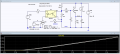
If you're reverting to a generic opto, perhaps the circuit below would keep the FL5150 happy. Current draw is only ~500uA, the response is substantially independent of the 10uA current source, D-ctrl goes down to ~50mV and linearity is good for a duty cycle in the 15%-100% range. Q1 is used as a voltage follower for the smoothed PWM voltage from the opto output, but its Vbe does introduce a slight temperature dependence as seen in the curve plots.
IsolatedPWM3.png
 

Thread Starter

mriksman

Joined Aug 31, 2010
113
Sorry. I gave you the wrong asy file. Here's (hopefully!) the right one.

Strange indeed. That FL certainly seems a very fussy IC. Perhaps there's enough capacitance somewhere that causes D-ctrl to get pulled down to ~0V at power-up, so the IC goes into low power mode? I don't see anything in the datasheet to suggest that low power mode is a latched function though.

Edit:
What voltage is on the Vs and OCS pins?
What values are your C1,2,3 caps and R1 (as per the datasheet) ?
Awesome. It works now. I tested a practical circuit and verified the results;
1591265326534.png
What is frustrating, is that it has the same performance as a normal optoisolator (the left side).


The FL5150 certainly is fussy. But, Vdd was never meant to source current, so can't say I'm surprised...

It comes out of low power mode fine (slight delay). As long as the load resistor is high enough.

Vss is 16.2V (to GNDA).
Not sure where you want me to measure OSC1 and OSC2 referenced to? They go into a op-amp internally in the FL5150. I have set the Rsense resistors to 820k - so it will cut out about 240W (according to my calculations and choice of MOSFET)

C1 is 100nF
C2 is 4.7uF
C3 is 100nF
R1 is 33k


The FL5150 with its 10uA current on DIM Control was designed to work with a potentiometer. Or perhaps a digital potentiometer. They also mention a 0-10V signal and using a 4:1 voltage divider. But as the GND of each FL5150 must be independent, then so does the DIM control reference/GND.
 

Attachments

Alec_t

Joined Sep 17, 2013
15,156
Since you have the opamp as a buffer, you could increase those RL values considerably (hence reduce the Vdd load) if necessary/advantageous.
 

Thread Starter

mriksman

Joined Aug 31, 2010
113
Since you have the opamp as a buffer, you could increase those RL values considerably (hence reduce the Vdd load) if necessary/advantageous.
Can't, because it effects the PWM waveform which is noticeable at lower and higher duty cycles;
1591413091018.png
 

fastbike

Joined Dec 29, 2020
128
Thanks for the discussion here, I'm looking to do something similar, but as a quad channel dimmer controlled by a micro controller.
From what I can see the PWM inputs are still not isolated to the full spec of the MOCD217R2M (see https://www.onsemi.com/products/opt...ut---dc-sensing-input-optocouplers/mocd217r2m) because the feedback loop runs from the output side to the input side. My understanding is the input and output should be be clearly separated to achieve clearance/creepage requirements.
Are your PWM inputs generated from a source which is isolated from user contact and/or true ground ?
 

fastbike

Joined Dec 29, 2020
128
That is a great suggestion. I can't find the pins in the schematic on the CD4103B datasheet, but are the pins PRE the same as SET, and the CLR the same as RESET ?
 
Top