Facebook
 Google
 GitHub
 Linkedin
Recently, I created an interposer module to translate the 168 pins (486 socket) of a Texas Instruments TI486SXL2-G66 to that of a 132 pin socket (386). From what I could discern after reading the TI486SXL Reference Guide, found here: https://archive.org/details/bitsavers_tiTI486199XLMicroprocessorsReferenceGuide_19799789 , the TI486SXL2 PGA168 should be the same as the QFP144 and PGA132 variants with minor exceptions. QFP144 and PGA168 have the FLUSH circuits built-in (although you do not have to use them if you don't wire up MEMW#), they have a FLT#, which can be left floating as it contains a built-in pull-up resistor, they run at 3.6 V, and have a few more GND (Vss) and voltage (Vcc) pins. Otherwise, the TI486SXL2 PGA168 is the same as the PGA132 unit which is intended to plug directly into a 386 motherboard's socket. I have the PGA 132 SXL2-50 5V chip and it works perfectly in all my 386 motherboards. The issue is that the PGA132 units only went up to 50 MHz, while the PGA168 and QFP144 variants went up to 66 MHz at 3.6 V. The TI486SXL2-66 chips in PGA168 format are readily obtainable new for $15 and would make for the ultimate 386 upgrade chip.
A CPU upgrade company did produce QFP144 units on a PGA132 interposer, but they are nearly impossible to find now. This is essentially what I am trying to do, but with using the PGA168 unit on a PGA132 interposer board with a voltage regulator module set to 3.6 V. Considering how much the SXL2-66 upgrade QFP144 sold for recently on eBay, I figured there might be interest in creating an interposer board for the more common TI486SXL2-66 PGA168. I planned to start with a proof of concept prototype, then possibly create a proper PCB if there was sufficient interest on the vintage and classic computer forums.
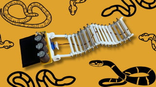
Here is an image of my prototype

And here is an image of the unit an upgrade company produced back in the day.

Here is an image of the 486SXL2 in the PGA132 variant, but limited to 50 MHz at 5V.

I built the prototype using a snap-able solder boards, a MIC29302WT (LDO = 0.37V @ 3A), 10 uF cermaic input cap, 10 uF tantalum output cap, a resistor, a trimmer, and solid core 24, 28 & 30 AWG wire. I tested several linear and switching voltage regulators before deciding on the MIC29302WT. I finished the prototype after about 10 days of casual soldering using the pinout translation scheme found in the TI486SXL reference manual, as shown below. The exception is that the Vcc pins on the PGA168 side get wired to the output of the voltage regulator instead of the 5 V line from the PGA132 side (the motherboard). I have the trimmer set such that the voltage to the CPU is 3.60 V. I confirmed this after the prototype was powered on in the motherboard.

Unfortunately, I could not get the prototype to work in any of my 386 motherboards, that is, when installed and the motherboard powered on, nothing is displayed on the monitor. In each motherboard, the TI486SXL2-50 PGA132 CPU worked fine though. I have checked each solder connection three times now and also confirmed that none of the wires shorted to any additional pins, e.g. while soldering some pin, the cladding on an adjacent wire melts and unintentionally causes bare wire to touch. Perhaps there could still be some cross-talk?
I noticed on the QFP144 upgrade module that there are some extra glue logic components, such as additional decoupling capacitors, a NOR gate, and a PAL. I do not see how these glue logic components would be necessary though because the SXL2-50 PGA132 works fine in my motherboards. I have come across many 486 upgrade interposer boards which also contain programmable logic device, such as PALs or GALs, and gate circuits. On many motherboards, these were not required. I believe that they are often added to increase cross compatibility with various systems, mostly archaic or non-standard motherboards. Could there be some other difference between the PGA168 and PGA132 SXL2 chips that has eluded me? I also suspect the glue logic on this unit writes to the CCR0, bit6 register, thereby putting the CPU into clock-double mode.
My gut feeling is that there is something very fundamental I have overlooked. The TI486SXL2 reference manual, at least the one I could find online, does not specifically list the 66 MHz variants of the processor, neither in the PGA168, nor the QFP144 formats. Without an updated reference manual, I cannot verify if any minor changes were made with the 3.6 V version of the TI486SXL2, however it seems unlikely. Does anyone here have a reference manual which mentions the TI486SXL2 - 66 CPU?
I am aware that my prototype is lacking some decoupling capacitors for the 3.6 V bus, that is, aside from the 10 uF capacitor I soldered on at the output of the voltage regulator module. My module has two strips of 3.6 V Vcc that I used to connect all the Vcc pins to - one on the top, and one on the bottom of the interposer. Below is an image of the noise at Vcc to GND using a budget 100 MHz oscilliscope I have.

There is about 200 mV of noise around the set voltage of 3.6 V. I then added a 100 uF X5R ceramic capacitor to one of the 3.6 V buses, but the noise, as viewed on the scope, did no change. In my experience, 200 mV of noise on the Vcc pin hasn't prevented any of my 486-class CPUs from functioning. While it is normally preferred to have a decoupling capacitor right at the Vcc pin before going into the CPU I have doubts that this will correct my problem at hand. There are 23 Vcc pins. I'm concerned that going to such trouble to solder SMD caps to these 23 pins will not help and cause endless frusturation. I have some IBM 5x86c-100HF interposer boards. They contain about 2 dozen decoupling capacitors. On one unit, I removed all the capacitors; on the other unit, I left them on. After extensive tests, even at overclocked frequencies of 133 MHz on a 66 Mhz bus, both units performed equally stable from my visual perspective or running demanding software in loop (e.q. Quake). However, if the experts think the issue is with not having decoupling capacitors on every Vcc pin, please let me know and I will try to get them added. What capacity? Would 0.1 uF ceramics do it?
I have three of these TI486SXL2-66 CPUs and I tried them all - the results was the same. I also tried setting FLT# to ground at startup and also to set FLT# to GND after power-up, but the result was the same. FLT# is for floating the bus signal. FLT# and MEMW# are the only two pins on the QFP144 and PGA168 chips which are not on the PGA132. I do not really understand what FLT# does, but I will copy/paste here what the reference manual says about it.
FLT#
Float (active low). This input forces all bidirectional and output signals to a 3-state condition. Floating the signals allows the microprocessor signals to be driven externally without physically removing the device from the circuit. The microprocessor must be reset following assertion or deassertion of FLT#. This signal may be used in conjunction with an upgrade socket. FLT# is internally connected to a pullup resistor to prevent it from floating active when left unconnected.
Elsewhere in the reference manual, it is noted that FLT# should only be used for testing purposes, so I think it is safe to ignore this pin. The other pin is,
MEMW#
Memory Write (active low). This input is used in the cache interface logic which flushes the cache in systems that hold the CPU during DMA and MASTER cycles.
MEMW# is the pin which leads to the hardware flush circuit (NAND gate and an inverter) inside the PGA168 and QFP144 chips. You connect MEMW# from the motherboard's ISA bus to MEMW# on the CPU. This is why the prototype has a single header. Anyway, the motherboard I'm testing already has this circuit built in, so this pin is redundant. The motherboard's circuit drives FLUSH# directly, which performs the same function. Connecting or not connecting this pin will not prevent the motherboard from powering up. I've tried it connected and unconnected.
I tested the prototype using 50, 66, and an 80 MHz oscillators. Keep in mind that on 386 motherboards, the CPUs run at 1/2 CLK2, so when using a 50 MHz oscillator, the CPU is running at 25 MHz. If there were cross-talk issues, I figured running the CPU at 25 MHz would have at least showed signs of life; it did not. I have a 33.33 MHz oscillator on order to try running the CPU at 16 MHz to see if this helps. Note that for the CPU shown to run at its full rated speed of 66 MHz, one would have to set a register in the CPU to clock doubling mode (there is no CLKMUL like on traditional 486 CPUs). This is what one must do to get the TI486SXL2-50 running at 50 MHz instead of the 25 MHz bus speed.
The average length of the wires is around 2", or about 50 mm. Some are only 1/2", while I think the longest might be 3". I am testing with a 50 Mhz osc, so the CPU is running at 25 MHz. For the communication lines, I used 30 AWG, which according to google, is 0.254 mm. For the average condition, the website listed below indicates an impedance at 0.086 + j 9.0 ohms. Do you think this is an issue? And that I should be impedance matching these 30 AWG transmission lines?
http://chemandy.com/calculators/round-wire-impedance-calculator.htm
I tried to make each wire as short as possible while still being able to solder the joints. Given the length of wires and frequency, I have deduced from the information contained in the following link that I shouldn't need to impedance match to get my prototype working,
https://superuser.com/questions/942971/what-frequency-does-impedance-matching-become-important
However, if someone here seems to think this is critical to getting the chip to power-up, which components (R, L, C?) and values would be required and where?
I tested the motherboard with MR BIOS and the original AMI BIOS. I tested with the FPU installed, removed, and with the co-processor jumper set to off. Still no signs of life. Keep in mind that the Texas Instruments 486DLC, 486SXL and 486SXL2 are arcitecturally 386 CPUs but have added L1 cache and the 486 instruction set. So I cannot merely install my 486SXL2 into a 486 motherboard and have it work. The 486SXL reference guide does go over the few changes that a motherboard needs to be aware of in Appendix D. I have never seen a 486 motherboard manual with specific support for the PGA168 version of the 486SXL2 and it makes me wonder why TI even bothered making them. I guess they must have offered a substantial price benefit over the Intel 486SX, but what OEM's were producing boards for them?
Lastly, how would I go about troubleshooting this prototype without a logic analyser, that is, just using a 2-channel 100 MHz oscilliscope and a multi-meter? When I still had the 66.666 MHz oscillator installed in the board (I now have the 50 MHz piece), I took a screenshot of the CLK2 signal and of the Address line, A2. What should I be looking for on each CPU pin and in what order following a reset (or power on)? Is anyone here knowedgable enough to walk me through this process?
CLK2 looks OK as far as I can tell, it is 66.6 MHz (meaning the CPU is running at 33.3 MHz). A2 is about 0 V, but will shoot up to 3.6 V when you hit the reset button on the motherboard, then back down to 0. I did not check address 1 or 2, because, according to the reference guide, it seems address 0 is derived from the Byte Enable output pins and some boolean algebra, whereby A0 = (BE0# · BE2#) + (BE0# · BE1#) and A1 = BE0# · BE1#, so I checked the next lowest order address, which is A2.

The basic input and outputs from the TI486SXL2 can be found from this diagram

Any input leading to the successful operation of this prototype would be greatly appreciated.
A CPU upgrade company did produce QFP144 units on a PGA132 interposer, but they are nearly impossible to find now. This is essentially what I am trying to do, but with using the PGA168 unit on a PGA132 interposer board with a voltage regulator module set to 3.6 V. Considering how much the SXL2-66 upgrade QFP144 sold for recently on eBay, I figured there might be interest in creating an interposer board for the more common TI486SXL2-66 PGA168. I planned to start with a proof of concept prototype, then possibly create a proper PCB if there was sufficient interest on the vintage and classic computer forums.
Here is an image of my prototype
And here is an image of the unit an upgrade company produced back in the day.
Here is an image of the 486SXL2 in the PGA132 variant, but limited to 50 MHz at 5V.
I built the prototype using a snap-able solder boards, a MIC29302WT (LDO = 0.37V @ 3A), 10 uF cermaic input cap, 10 uF tantalum output cap, a resistor, a trimmer, and solid core 24, 28 & 30 AWG wire. I tested several linear and switching voltage regulators before deciding on the MIC29302WT. I finished the prototype after about 10 days of casual soldering using the pinout translation scheme found in the TI486SXL reference manual, as shown below. The exception is that the Vcc pins on the PGA168 side get wired to the output of the voltage regulator instead of the 5 V line from the PGA132 side (the motherboard). I have the trimmer set such that the voltage to the CPU is 3.60 V. I confirmed this after the prototype was powered on in the motherboard.
Unfortunately, I could not get the prototype to work in any of my 386 motherboards, that is, when installed and the motherboard powered on, nothing is displayed on the monitor. In each motherboard, the TI486SXL2-50 PGA132 CPU worked fine though. I have checked each solder connection three times now and also confirmed that none of the wires shorted to any additional pins, e.g. while soldering some pin, the cladding on an adjacent wire melts and unintentionally causes bare wire to touch. Perhaps there could still be some cross-talk?
I noticed on the QFP144 upgrade module that there are some extra glue logic components, such as additional decoupling capacitors, a NOR gate, and a PAL. I do not see how these glue logic components would be necessary though because the SXL2-50 PGA132 works fine in my motherboards. I have come across many 486 upgrade interposer boards which also contain programmable logic device, such as PALs or GALs, and gate circuits. On many motherboards, these were not required. I believe that they are often added to increase cross compatibility with various systems, mostly archaic or non-standard motherboards. Could there be some other difference between the PGA168 and PGA132 SXL2 chips that has eluded me? I also suspect the glue logic on this unit writes to the CCR0, bit6 register, thereby putting the CPU into clock-double mode.
My gut feeling is that there is something very fundamental I have overlooked. The TI486SXL2 reference manual, at least the one I could find online, does not specifically list the 66 MHz variants of the processor, neither in the PGA168, nor the QFP144 formats. Without an updated reference manual, I cannot verify if any minor changes were made with the 3.6 V version of the TI486SXL2, however it seems unlikely. Does anyone here have a reference manual which mentions the TI486SXL2 - 66 CPU?
I am aware that my prototype is lacking some decoupling capacitors for the 3.6 V bus, that is, aside from the 10 uF capacitor I soldered on at the output of the voltage regulator module. My module has two strips of 3.6 V Vcc that I used to connect all the Vcc pins to - one on the top, and one on the bottom of the interposer. Below is an image of the noise at Vcc to GND using a budget 100 MHz oscilliscope I have.
There is about 200 mV of noise around the set voltage of 3.6 V. I then added a 100 uF X5R ceramic capacitor to one of the 3.6 V buses, but the noise, as viewed on the scope, did no change. In my experience, 200 mV of noise on the Vcc pin hasn't prevented any of my 486-class CPUs from functioning. While it is normally preferred to have a decoupling capacitor right at the Vcc pin before going into the CPU I have doubts that this will correct my problem at hand. There are 23 Vcc pins. I'm concerned that going to such trouble to solder SMD caps to these 23 pins will not help and cause endless frusturation. I have some IBM 5x86c-100HF interposer boards. They contain about 2 dozen decoupling capacitors. On one unit, I removed all the capacitors; on the other unit, I left them on. After extensive tests, even at overclocked frequencies of 133 MHz on a 66 Mhz bus, both units performed equally stable from my visual perspective or running demanding software in loop (e.q. Quake). However, if the experts think the issue is with not having decoupling capacitors on every Vcc pin, please let me know and I will try to get them added. What capacity? Would 0.1 uF ceramics do it?
I have three of these TI486SXL2-66 CPUs and I tried them all - the results was the same. I also tried setting FLT# to ground at startup and also to set FLT# to GND after power-up, but the result was the same. FLT# is for floating the bus signal. FLT# and MEMW# are the only two pins on the QFP144 and PGA168 chips which are not on the PGA132. I do not really understand what FLT# does, but I will copy/paste here what the reference manual says about it.
FLT#
Float (active low). This input forces all bidirectional and output signals to a 3-state condition. Floating the signals allows the microprocessor signals to be driven externally without physically removing the device from the circuit. The microprocessor must be reset following assertion or deassertion of FLT#. This signal may be used in conjunction with an upgrade socket. FLT# is internally connected to a pullup resistor to prevent it from floating active when left unconnected.
Elsewhere in the reference manual, it is noted that FLT# should only be used for testing purposes, so I think it is safe to ignore this pin. The other pin is,
MEMW#
Memory Write (active low). This input is used in the cache interface logic which flushes the cache in systems that hold the CPU during DMA and MASTER cycles.
MEMW# is the pin which leads to the hardware flush circuit (NAND gate and an inverter) inside the PGA168 and QFP144 chips. You connect MEMW# from the motherboard's ISA bus to MEMW# on the CPU. This is why the prototype has a single header. Anyway, the motherboard I'm testing already has this circuit built in, so this pin is redundant. The motherboard's circuit drives FLUSH# directly, which performs the same function. Connecting or not connecting this pin will not prevent the motherboard from powering up. I've tried it connected and unconnected.
I tested the prototype using 50, 66, and an 80 MHz oscillators. Keep in mind that on 386 motherboards, the CPUs run at 1/2 CLK2, so when using a 50 MHz oscillator, the CPU is running at 25 MHz. If there were cross-talk issues, I figured running the CPU at 25 MHz would have at least showed signs of life; it did not. I have a 33.33 MHz oscillator on order to try running the CPU at 16 MHz to see if this helps. Note that for the CPU shown to run at its full rated speed of 66 MHz, one would have to set a register in the CPU to clock doubling mode (there is no CLKMUL like on traditional 486 CPUs). This is what one must do to get the TI486SXL2-50 running at 50 MHz instead of the 25 MHz bus speed.
The average length of the wires is around 2", or about 50 mm. Some are only 1/2", while I think the longest might be 3". I am testing with a 50 Mhz osc, so the CPU is running at 25 MHz. For the communication lines, I used 30 AWG, which according to google, is 0.254 mm. For the average condition, the website listed below indicates an impedance at 0.086 + j 9.0 ohms. Do you think this is an issue? And that I should be impedance matching these 30 AWG transmission lines?
http://chemandy.com/calculators/round-wire-impedance-calculator.htm
I tried to make each wire as short as possible while still being able to solder the joints. Given the length of wires and frequency, I have deduced from the information contained in the following link that I shouldn't need to impedance match to get my prototype working,
https://superuser.com/questions/942971/what-frequency-does-impedance-matching-become-important
However, if someone here seems to think this is critical to getting the chip to power-up, which components (R, L, C?) and values would be required and where?
I tested the motherboard with MR BIOS and the original AMI BIOS. I tested with the FPU installed, removed, and with the co-processor jumper set to off. Still no signs of life. Keep in mind that the Texas Instruments 486DLC, 486SXL and 486SXL2 are arcitecturally 386 CPUs but have added L1 cache and the 486 instruction set. So I cannot merely install my 486SXL2 into a 486 motherboard and have it work. The 486SXL reference guide does go over the few changes that a motherboard needs to be aware of in Appendix D. I have never seen a 486 motherboard manual with specific support for the PGA168 version of the 486SXL2 and it makes me wonder why TI even bothered making them. I guess they must have offered a substantial price benefit over the Intel 486SX, but what OEM's were producing boards for them?
Lastly, how would I go about troubleshooting this prototype without a logic analyser, that is, just using a 2-channel 100 MHz oscilliscope and a multi-meter? When I still had the 66.666 MHz oscillator installed in the board (I now have the 50 MHz piece), I took a screenshot of the CLK2 signal and of the Address line, A2. What should I be looking for on each CPU pin and in what order following a reset (or power on)? Is anyone here knowedgable enough to walk me through this process?
CLK2 looks OK as far as I can tell, it is 66.6 MHz (meaning the CPU is running at 33.3 MHz). A2 is about 0 V, but will shoot up to 3.6 V when you hit the reset button on the motherboard, then back down to 0. I did not check address 1 or 2, because, according to the reference guide, it seems address 0 is derived from the Byte Enable output pins and some boolean algebra, whereby A0 = (BE0# · BE2#) + (BE0# · BE1#) and A1 = BE0# · BE1#, so I checked the next lowest order address, which is A2.
The basic input and outputs from the TI486SXL2 can be found from this diagram
Any input leading to the successful operation of this prototype would be greatly appreciated.