Need Help Troubleshooting My First SMPS Design (220VAC to 12V 60W)

Thread Starter

Bora Fikret Karakütük

Joined Aug 29, 2017
16
Hi everyone,

I’m working on my first switch-mode power supply (SMPS) design. It’s supposed to convert 220V AC input to 12V DC at 60W output.

I’m not an electronics engineer and I don’t have formal training in this field – I’m just a hobbyist trying to learn.

The transformer was custom-wound by a manufacturer in China. Here are the specs:

Core: EE33

Primary Inductance: 82 µH

Primary: 15 turns, 0.65 mm wire

Secondary: 3 turns, 1.5 mm wire

Auxiliary: 5 turns, 0.2 mm wire

When I powered up the PCB for the first time, the transistor and Rsense resistors burned out instantly. I suspect my snubber/clamp circuit calculations might be wrong.

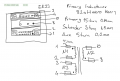
I’ve attached a hand-drawn diagram of my transformer (see image).

Could you please help me troubleshoot this design? I’d appreciate explanations in simple terms since I’m still learning.

Thank you very much!
 

Attachments

Irving

Joined Jan 30, 2016
4,996
Welcome to AAC.

Was this your own design, or from elsewhere? If yours, please post your calculations, else a link to the original source design.

Did you lay out the PCB yourself? Might be helpful to post the zipped gerber files for review.

For clarity your schematic doesn't show which variant of the UC384x smps controller you're using, nor your MOSFET. Please post that info.

What test gear do you have available? A decent cat III 600v multimeter is a minimum.

Obligatory safety reminder: Be very careful when touching anything on the 'hot' side. Only 1 hand in use at a time, and preferably using an isolation transformer and an RCD outlet. (Sorry if that sounds patronizing, but even experienced engineers get caught out - myself included!)

Before replacing the MOSFET and sense resistors, do a sanity check on voltages - what are D+ (+) to S (-) and pin 7 of the UC384x (+) to S (-)?
 

Pyrex

Joined Feb 16, 2022
501
At first glance, it seems that there should be more turns in the primary winding of the transformer.
Secondly, is there an air gap in the transformer?
Third, what are the specifications of the power transistor Q1?
RC circuit must be provided for the D8 power diodes.
It is unclear where the 5V voltage is coming from and how the optocoupler is connected.?

One more note - why did you choose the flyback topology? Choosing a forward topology makes it much simpler to make a transformer. Flyback is a widely used topology solely because it saves one inductor, but this is important only in mass production.
 

Thread Starter

Bora Fikret Karakütük

Joined Aug 29, 2017
16
Welcome to AAC.

Was this your own design, or from elsewhere? If yours, please post your calculations, else a link to the original source design.

Did you lay out the PCB yourself? Might be helpful to post the zipped gerber files for review.

For clarity your schematic doesn't show which variant of the UC384x smps controller you're using, nor your MOSFET. Please post that info.

What test gear do you have available? A decent cat III 600v multimeter is a minimum.

Obligatory safety reminder: Be very careful when touching anything on the 'hot' side. Only 1 hand in use at a time, and preferably using an isolation transformer and an RCD outlet. (Sorry if that sounds patronizing, but even experienced engineers get caught out - myself included!)

Before replacing the MOSFET and sense resistors, do a sanity check on voltages - what are D+ (+) to S (-) and pin 7 of the UC384x (+) to S (-)?
Thank you very much for your considerate and understanding reply. As someone who is doing this mainly as a hobby and for learning purposes, I truly appreciate the supportive tone.

I prepared all the calculations myself based on my own research from various sources on the internet; I did not use a ready-made design. I’ve attached my calculation file for reference, as well as the Gerber files for review.

Thank you again for taking the time to help – it means a lot for those of us learning as we go.
 

Attachments

Irving

Joined Jan 30, 2016
4,996
It is unclear where the 5V voltage is coming from and how the optocoupler is connected.?
From the Vref output of the UC384x controller.

The optocoupler is driven by the TL431; when output volts >12.5 the TL431 turns on, tyrning the LED on. Thus raises the voltage at FB (UC384x pin2) reducing the duty cycle.
 

Irving

Joined Jan 30, 2016
4,996
What MOSFET are you using, its not stated on the schematic or in the BOM...

A word of advice, please put the part identifiers eg R1, C1 on the silk screen and also orientation marks, such as pin 1 marker for U1 - otherwise troubleshooting the PCB is really hard work.

I think you're using a UC3844B controller though I couldn't find a specific reference to it. Is that right?

I like your design document, though this all looks far too formal for a 'homer' project (would have been nicer in English :D , but maths is universal!).
 

Thread Starter

Bora Fikret Karakütük

Joined Aug 29, 2017
16
First of all, thank you for your feedback on the document. Even as a hobby project, I make a point of documenting my work thoroughly so that I can learn from it and refer back when needed.

For the design, I configured it for 100 kHz PWM using either the UC3842, which allows 100% duty cycle, or the UC3844, which is limited to 50% duty cycle, depending on which controller I have on hand.

I have tested both the FQP6N80C and FQP6N60 MOSFETs, but unfortunately, both failed during operation.
 

michael8

Joined Jan 11, 2015
472
Instead of just powering it up and possibly blowing stuff again, I'd suggest testing sections at a time and checking
with an oscilloscope.

For instance, breaking the path on D+ after C3 so that Q1 has no power would allow testing the input AC to
DC path and checking C3 for the correct voltage. Of course, I'd expect this part to be working.

Then without the AC input, a separate limited current supply could be used to power the switching IC while
a (possibly different) low voltage source supplied the drain of Q1. This could be a low stress combination
to observe the switching and timing.
 

Irving

Joined Jan 30, 2016
4,996
Instead of just powering it up and possibly blowing stuff again, I'd suggest testing sections at a time and checking
with an oscilloscope.
And blowing up a 'scope as well - without an isolation transformer and/or a good differential probe, IMHO, this isn't a safe way to diagnose faults for a beginner, though I agree that taking it in sections is the right way to approach it, and I do take your point about using a low-voltage supply - which assumes the TS has a suitable bench supply etc. Looking at the PCB with all SMD parts and extremely compact, it could actually be quite hard to break out the necessary connections. Given the catastrophic nature of the fault, I'd suggest there's a more fundamental issue...
 

Irving

Joined Jan 30, 2016
4,996
First of all, thank you for your feedback on the document. Even as a hobby project, I make a point of documenting my work thoroughly so that I can learn from it and refer back when needed.

For the design, I configured it for 100 kHz PWM using either the UC3842, which allows 100% duty cycle, or the UC3844, which is limited to 50% duty cycle, depending on which controller I have on hand.

I have tested both the FQP6N80C and FQP6N60 MOSFETs, but unfortunately, both failed during operation.
I have some good news and, sorry, some bad news...

The good news is that, fundamentally there's nothing wrong with your design. I have some minor issues with a couple of component values, but it'll work.

The bad news is your PCB layout is wrong. To be fair, you've fallen foul of a little quirk of KiCAD (and I have as well in the past, so if its any consolation, you're not the first).

The problem is, like many, you've designed your schematic, and while drawing you've wanted an NMOS MOSFET. So you logically pick the NMOS MOSFET symbol at the top of the list (even though it says its for spice simulation); how do I know this - because the pins are labelled D,G,S and not 1, 2, 3. If you'd picked the one lower down, Q_NMOS_GDS you'd have been fine. Unfortunately the default pin numbering for the 1st symbol is 1=D, 2=G, 3=S, which is true for many low-power MOSFETs but never for a power package such as TO-220, TO-247, etc where the centre pin and the tab is always the drain. ie 1=G, 2=D, 3=S. So when you attached the TO-220 footprint to the symbol, boom! See illustration below. As a learning exercise, this is the hard way - always check the the pin numbering in the footprint and cross-check with the datasheet - and then check it again a few days later... I wouldn't hold out too much hope for the controller chip either...

1756313312503.png1756313992497.png
 

michael8

Joined Jan 11, 2015
472
And running from a current limited low voltage (15V?) supply would not be likely to blow anything out but would likely
so some very obvious wrong behavior...
 

Thread Starter

Bora Fikret Karakütük

Joined Aug 29, 2017
16
I have some good news and, sorry, some bad news...

The good news is that, fundamentally there's nothing wrong with your design. I have some minor issues with a couple of component values, but it'll work.

The bad news is your PCB layout is wrong. To be fair, you've fallen foul of a little quirk of KiCAD (and I have as well in the past, so if its any consolation, you're not the first).

The problem is, like many, you've designed your schematic, and while drawing you've wanted an NMOS MOSFET. So you logically pick the NMOS MOSFET symbol at the top of the list (even though it says its for spice simulation); how do I know this - because the pins are labelled D,G,S and not 1, 2, 3. If you'd picked the one lower down, Q_NMOS_GDS you'd have been fine. Unfortunately the default pin numbering for the 1st symbol is 1=D, 2=G, 3=S, which is true for many low-power MOSFETs but never for a power package such as TO-220, TO-247, etc where the centre pin and the tab is always the drain. ie 1=G, 2=D, 3=S. So when you attached the TO-220 footprint to the symbol, boom! See illustration below. As a learning exercise, this is the hard way - always check the the pin numbering in the footprint and cross-check with the datasheet - and then check it again a few days later... I wouldn't hold out too much hope for the controller chip either...

View attachment 354917View attachment 354918
Sir,

Thank you immensely for dedicating your time and expertise to diagnosing the issue.
After spending so much effort on calculations and design without being able to get it to work, I had honestly started to lose hope.

Your fine touch means a lot to me. I do not expect to design a professional-grade SMPS, and there will be no commercial gain from this project – in fact, I will have to spend money to turn it into a product. But I enjoy adding value to myself through such work, which is truly the field of engineers like you.

I have the utmost respect for you, and I deeply appreciate the fact that you offered your help without any hint of arrogance.

Thank you.
 

ronsimpson

Joined Oct 7, 2019
4,645
When I first power up a new supply:
Use a bench supply to power the PWM. Look to see if the oscillator is working. Look for Gate Drive.
Use a current limited second bench supply to power up the "line voltage". Maybe start out at 12V or 0V. With only a small voltage check to see that the phase is right on the transformer. Slowly bring up the volts. You can stack several supplies to get higher voltage.
I have 200V and also 400V supplies for testing like this. I also sometime use a variable transformer so I can change the input voltage from 0 to line voltage. Many of the variable transformers do not have isolation, some do. If you do this much you might want to get an isolation transformer. They can save your life and make probing with a scope safe. I have isolation transformers with 120/220 inputs and 120/220 outputs.
1756654260328.png
 

ronsimpson

Joined Oct 7, 2019
4,645
If you have problems with the error amplifier, please check the way you have U1-pin2 connected to U2-pin3. It might work but I normally have a 10K resistor or some resistance in that connection. There is more than one way to do this error amp.
 

Irving

Joined Jan 30, 2016
4,996
If you have problems with the error amplifier, please check the way you have U1-pin2 connected to U2-pin3. It might work but I normally have a 10K resistor or some resistance in that connection. There is more than one way to do this error amp.
You're right, I hadn't spotted that. Its normally a 4k7 or 4k99 on most reference designs. The resistor is needed at the input to the error amp.
 

Ian0

Joined Aug 7, 2020
13,097
1. I would have expected about 10 times as much primary inductance.
60W input would be an average of 184mA at 325V DC. Peak is approximately 6x average for a flyback converter. That gives a peak current of 1.1A. Say about 2.5us on time, That gives dI/dt = 44300 A/s. At 325V supply L=V/(dI/dt) = 733uH.
2. An efficient transformer would need a sandwich design - From the inside out-> Half of primary, Secondary, rest of primary, auxiliary.
3.You have compensation on the TL431, then you have MORE compensation on the UC3842, each of which contributes 90° of phase shift. Add in the parasitics and you have at least 180° of phase shift in the error amplifier, so you don't have an error amplifier, you have an error oscillator. The UC3842's error amplifier has an output current that is limited to 800uA, so force the output high by connecting FB to ground, and use the output as a constant current source. Then connect the opto between COMP and 0V.
This is a really good paper on error amplifiers.
 

Thread Starter

Bora Fikret Karakütük

Joined Aug 29, 2017
16
1. I would have expected about 10 times as much primary inductance.
60W input would be an average of 184mA at 325V DC. Peak is approximately 6x average for a flyback converter. That gives a peak current of 1.1A. Say about 2.5us on time, That gives dI/dt = 44300 A/s. At 325V supply L=V/(dI/dt) = 733uH.
2. An efficient transformer would need a sandwich design - From the inside out-> Half of primary, Secondary, rest of primary, auxiliary.
3.You have compensation on the TL431, then you have MORE compensation on the UC3842, each of which contributes 90° of phase shift. Add in the parasitics and you have at least 180° of phase shift in the error amplifier, so you don't have an error amplifier, you have an error oscillator. The UC3842's error amplifier has an output current that is limited to 800uA, so force the output high by connecting FB to ground, and use the output as a constant current source. Then connect the opto between COMP and 0V.
This is a really good paper on error amplifiers.
Thank you for your detailed feedback. I truly appreciate the time you took to analyze my design.


Regarding the primary inductance (Lm):


  • My design is intentionally DCM (Discontinuous Conduction Mode) at 100 kHz with 60 W output, operating from a universal AC input (85–265 VAC).
  • Under these conditions, the calculated inductance comes out to approximately 82 µH, which matches the energy-based formula:
  • Lm = (Vdcmin * Dmax)^2 / (2 * Pin * fs)

    Lm = (71.27 * 0.47698)^2 / (2 * 70.6 * 100000)
    Lm ≈ 81.8 uH

  • resulting in 81.8 µH.

Your 733 µH estimation seems to assume a CCM (Continuous Conduction Mode) design with a different Ton and peak current profile, which would naturally require a much larger magnetizing inductance.


I agree with your other points:


  • Sandwich winding is an excellent idea to reduce leakage.
  • Compensation should be carefully reviewed to avoid excess phase shift – I will analyze my feedback loop again to ensure stability.

Thank you once again for the valuable input!
 
Top