Facebook
 Google
 GitHub
 Linkedin
Hello all,
I'm designing my first half bridge boost converter and I've got these two problems:
Any help would be appreciated
I'm designing my first half bridge boost converter and I've got these two problems:
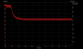
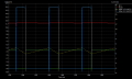
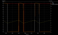
- These transients that appear no matter what simulation model of MOSFET I use. I've got these massive spikes. They even appear when I insert larger diodes onto the MOSFETs. Is this an artifact of the simulation? 10 ns step time and a 2 ms simulation, if it helps. I've heard that switching mode converters are hard to simulate.
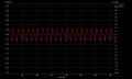
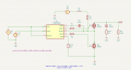
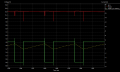
- My output voltage doesn't have any ripple. My professor pointed this out to me. Upon further thinking, this isn't a traditional boost converter I'm used to working with. The output follows the Phase pin output when high. I don't think I'm supposed to have an output ripple. I've attached the driver I'm using. I can't find any examples of the output voltage of this sort of converter online to confirm my second point.
Any help would be appreciated
Attachments
-
 23.5 KB Views: 12
 -
 27.5 KB Views: 12
 -
 31.1 KB Views: 9
 -
 26.7 KB Views: 8
 -
2 MB Views: 3