 Facebook
 Google
 GitHub
 Linkedin
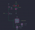
I want to make sure that on my development board, the guys can control loads through the logic level MOSFET or alternatively use the pin as a GPIO for serial data.
I have these issues and can't decide:
Thank you in advance for your help.
I have these issues and can't decide:
- 1. If I use a buffer before the jumper, when the voltage is shifted, RDS(on) will also change, and I want the MOSFET to always work at a VGS voltage of 5V.
- 2. If I use the buffer after (as shown in the attached circuit), the GPIO pin is not protected by the buffer and I cannot make the MOS work at 5V. Does anyone have any ideas on how to optimize the architecture topology?
Thank you in advance for your help.
Attachments
-
 35.7 KB Views: 8


