Gate Drive Waveform

Thread Starter

urb-nurd

Joined Jul 9, 2014
269
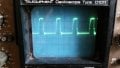
Hey guys, i am posting this just to make sure the gate drive waveform is ok.

I am currently driving one MOSFET with the gate drive circuit but plan to add a second, so i expect my rise time to change when i am charging twice the gate capacitance.
The PWM frequency i am using for switching is 25Khz.

Anyway, the switch on appears to be fast enough, the rise to the miller capacitance plateau appears near vertical.
Though, i am wondering if the switch off time is OK. It appears that it takes longer to discharger the miller capacitance than it takes to charge it.
The datasheet does say that that the switch off delay is three times the magnitude of the switch on delay.
The gate drive is an fod3180 gate drive optocoupler, so the gate is being pulled down at turn off.
My fet gets rather hot at low PWM duty ( i will definitely need to heat sink it) and i am just wanting to clarify that the gate drive isn't causing the temperature rise at low duty.
 

Attachments

crutschow

Joined Mar 14, 2008
34,470
Is that the transistor drain output?
The MOSFETs shouldn't get warm unless there is a significant load.
Post your circuit diagram.
 

Thread Starter

urb-nurd

Joined Jul 9, 2014
269
Thats the gate drive waveform of my FET, the scope is connected across the gate and the source.

The load is significant, i definitely expect heating of the fet due to the load current (inrush at least 50A, steady state current draw around 7A).
However when testing, i noticed the heat rose quicker with low duty cycles than it did with the duty at 100%.
The shematic is much the same as this:

But the gate drive opto is being supplied by a 12V zener and a capacitor rather than the dc-dc buck seen above.
Also, i have a 46 ohm resistor in series with the gate and another 720k from the gate to the ground.
 

crutschow

Joined Mar 14, 2008
34,470
If the load is a lamp, it will draw more peak current at low duty cycles.

Post the waveform at the drain. Particularly note the voltage when the MOSFET is ON.
 

Thread Starter

urb-nurd

Joined Jul 9, 2014
269
If the load is a lamp, it will draw more peak current at low duty cycles.

Post the waveform at the drain. Particularly note the voltage when the MOSFET is ON.
Come to think about it, i ruled out the fact that the peak current will be noticeable higher at lower duty as i assumed the thermal time constant of the filament would prevent the resistance from changing drastically.
Keyword: Assumed.
 

crutschow

Joined Mar 14, 2008
34,470
Come to think about it, i ruled out the fact that the peak current will be noticeable higher at lower duty as i assumed the thermal time constant of the filament would prevent the resistance from changing drastically............
Even if the filament has a long time constant, its resistance goes down as the average current and filament temperature go down.
 

Thread Starter

urb-nurd

Joined Jul 9, 2014
269
Even if the filament has a long time constant, its resistance goes down as the average current and filament temperature go down.
Indeed, but the larger the thermal time constant - the longer it takes to cool, thereby keeping the resistance at a higher level for longer(for a given prior high temperature).

I think we are saying the same thing haha.

Here is the waveform across the drain and source.

This is with the duty around 50% (i cant really remember).
The image shows the output of the rectifier in essence.
The switching frequency is too high to make out the dots constituting the pulsed dc waveform.
I noted the drain source voltage through varying duty cycles and saw what i guess i expected:
At 100% duty VDS = 24.5 mV
As i raise the duty, the voltage seen across drain and sources rises as function of the average between 24.5mV and 30+V.
What did you expect to see crutschow?
Maybe i misunderstood your request.


Also, heres a curious observation.
The image below shows the output of the rectifier when the duty cycle is 0, it seems the dc level of my capacitor is creeping past my diode every second pulse (from the rectifier output).


When i raise the duty level to 1 or 0.004%, the bridge output is as expected.

It seems as if the diode on the output of the rectifier is leaking back when the input to the rectifier goes negative.
I have absolutely no idea why this is remedied when the duty is incremented by 0.04%!
This isn't causing me any issues, but i am intrigued to investigate what is going on.
 

crutschow

Joined Mar 14, 2008
34,470
What I'm interested in seeing is the high frequency switching waveform at the drain.
Show a few cycles of that at the maximum point in the sinewave.
 

ronv

Joined Nov 12, 2008
3,770
Even with a really good FET like an IRFB4110 :D at 50 amps it will dissipate 10 watts for 10% of the time so like 1 watt. Add a little bit for switching losses and you might have 90 to 100C.
A small heat sink would probably make it much happier.
 

Thread Starter

urb-nurd

Joined Jul 9, 2014
269
Even with a really good FET like an IRFB4110 :D at 50 amps it will dissipate 10 watts for 10% of the time so like 1 watt. Add a little bit for switching losses and you might have 90 to 100C.
A small heat sink would probably make it much happier.
Sorry to be a pain, but could you explain how you got the 10W for 10% numbers?
Also, are there any recommendable heat sinks? i cant say i have looked into mosfet heatsinks ever.
Though i shall start!
Thanks for the input guys
 

kubeek

Joined Sep 20, 2005
5,795
10W comes from the Rdson and current, 50*50*0.0045 gives about 11W. Not sure what Ron meant with the 10%, I´d say that the mosfet will on average dissipate quite a bit more than just the 11W because of switching losses.
 

Thread Starter

urb-nurd

Joined Jul 9, 2014
269
10W comes from the Rdson and current, 50*50*0.0045 gives about 11W. Not sure what Ron meant with the 10%, I´d say that the mosfet will on average dissipate quite a bit more than just the 11W because of switching losses.
the 50A was my estimation of the inrush current.
The steady state current is around 6.25A (150W bulb, at 24V - I = P/V = 150/24 = 6.25A).
Though, every time the filament cools and i switch the fet on, i will see another inrush.
So if the on resistance is 0.0045Ω, and steady current is lets say 10A to obeverstate the power.
P = (10^2) * 0.0045 = 0.45W
I measured my bulb cold resistance to be 0.5 Ω.
So the inrush theoretically can reach (25√2)/0.5 = 70.1A
So max dissipation for the inrush is around 22.11W.

Theoretically, at low duty cycles i will be seeing peak currents between 10A and 70A.
Though i think this is likely going to be much lower than 70A.

Another question: I am going to hook up a second fet today to allow AC to pass through two fets in series.
The power dissipation across the body diode has me concerned.
Its forward voltage is 1.3V, given the drain current will vary from 10A+, i expect to dissipate around 13W every cycle.
IS this correct?
 
Last edited:

ronv

Joined Nov 12, 2008
3,770
Sorry, I guess I didn't explain that very well. :oops:

I was thinking a 10% duty cycle. So the voltage across the lamp will only be 2.5 volts RMS. It's hard to say what the lamp resistance will be, but probably still pretty low, so the loss in the FET will be pretty high since it is I squared x R even though it is only on for 10% of the time.
Does it glow at low duty cycle?
Hook the FETs in parallel not series. But a heat sink is probably cheaper.
 

ronv

Joined Nov 12, 2008
3,770
Indeed, but the larger the thermal time constant - the longer it takes to cool, thereby keeping the resistance at a higher level for longer(for a given prior high temperature).

I think we are saying the same thing haha.

Here is the waveform across the drain and source.

This is with the duty around 50% (i cant really remember).
The image shows the output of the rectifier in essence.
The switching frequency is too high to make out the dots constituting the pulsed dc waveform.
I noted the drain source voltage through varying duty cycles and saw what i guess i expected:
At 100% duty VDS = 24.5 mV
As i raise the duty, the voltage seen across drain and sources rises as function of the average between 24.5mV and 30+V.
What did you expect to see crutschow?
Maybe i misunderstood your request.


Also, heres a curious observation.
The image below shows the output of the rectifier when the duty cycle is 0, it seems the dc level of my capacitor is creeping past my diode every second pulse (from the rectifier output).


When i raise the duty level to 1 or 0.004%, the bridge output is as expected.

It seems as if the diode on the output of the rectifier is leaking back when the input to the rectifier goes negative.
I have absolutely no idea why this is remedied when the duty is incremented by 0.04%!
This isn't causing me any issues, but i am intrigued to investigate what is going on.
It is probably the leakage current of the diode .
 

Thread Starter

urb-nurd

Joined Jul 9, 2014
269
It is probably the leakage current of the diode .
Agreed, but why does the diode no longer leak with Pwm duty is only 0.04%?
When i raise the duty, the diode will pass forward current again to charge the caps and gate, little makes it through the load or fets at this duty level.
Is the minuscule forward current enough to prevent reverse current?
Also, why is the leakage present for alternating pulses?

I have changed my layout since earlier to incorporate two FETS to pass AC.


The schematic above works well aside from one issue: when the supply goes positive, the current through the zener passes through the body diode to the voltage supply.
So my lower Fet heats up more than the upper FET, can anyone recommend a solution to this?

When i use my scope to see the supply waveform with this lay-out, i still see leakage through D1 - even when i try another diode (same type however).
 

ronv

Joined Nov 12, 2008
3,770
Sorry, I can't explain the strange waveform. Maybe someone else has some ideas.
In your schematic the bottom FET never turns on the current is all thru the body diode so the power is I X E, with E being over a volt at high current.
Why would you want to do it this way?

Edit:
I think it is just stray capacitance holding the voltage up when you are not drawing any current. Kind of like adding a very small filter cap to the output of the bridge. Once the voltage from the bridge drops below 12 volts the diode to the 12 volt supply becomes forward biased and keeps the voltage from going below 11.6 or so.
You could add a large resistor, say 10k from the bridge to ground and it would look like you expect it to look.
 
Last edited:

Thread Starter

urb-nurd

Joined Jul 9, 2014
269
Sorry, I can't explain the strange waveform. Maybe someone else has some ideas.
In your schematic the bottom FET never turns on the current is all thru the body diode so the power is I X E, with E being over a volt at high current.
Why would you want to do it this way?

Edit:
I think it is just stray capacitance holding the voltage up when you are not drawing any current. Kind of like adding a very small filter cap to the output of the bridge. Once the voltage from the bridge drops below 12 volts the diode to the 12 volt supply becomes forward biased and keeps the voltage from going below 11.6 or so.
You could add a large resistor, say 10k from the bridge to ground and it would look like you expect it to look.
Im getting a little lost now, You say the lower FET never turns on and only functions with its body diode?
The gates of both FETS are connected together, so when the upper FET is on so is the lower one.
They both are used to pass my AC load waveform, while one FET is OPEN and biased so as to conduct normally, the other is configured to conduct via the body diode.
This way one device is in control per cycle, with the other using its body diode to permit a route for current.

In the circuit above i am not using a bridge rectifier anymore, i have removed it for AC operation. The voltage source is 25V rms AC.

The schematic above works pretty well, though the lower fet heats up more than the upper FET.
I think this is due to a path existing between the +ve and -Ve terminal through the body diode of the lower FET.
I think current flows through D1, then through the schottky D3 - through the 680 resistor and down through the zener. This then makes its way through the body diode of the lower FET M4 and back to the supply.
I think this may be causing my Lower FET to heat more than the upper one.
Any thoughts on this explanation?
 

RamaD

Joined Dec 4, 2009
328
The current thro' M4 body diode from that 680Ohms is 33mA (23V/680, assuming no drop across D3 and 35V on C2). That can only produce ~40mW to make any perceptible difference IMHO.
 

Thread Starter

urb-nurd

Joined Jul 9, 2014
269
The current thro' M4 body diode from that 680Ohms is 33mA (23V/680, assuming no drop across D3 and 35V on C2). That can only produce ~40mW to make any perceptible difference IMHO.
You are correct. I was trying to simulate the circuit to determine the current on LTspice but had all sorts of issues with timebase being to small and taking too long to draw the traces of my simulations.
What else could be the culprit?
The circuit seems to work as expected when i use it.
The voltages across the drain and source of both FETS are equal.
I might have a look and make sure there isnt any sources of stray inductance on one fet but not the other.
I guess that could cause some dissipation issues.
 

RamaD

Joined Dec 4, 2009
328
I just noticed the MBRS diode. These schottky barrier diodes are with low forward drop, but high reverse leakage current. That probably explains the waveform. Maybe not. How the second one?
 
Last edited:
Top