 Facebook
 Google
 GitHub
 Linkedin
Hi everyone,
New face here, I’ve been developing a replacement PCB for the original Nintendo Famicom RF modulator.
It plugs into the existing 7-pin ribbon cable and replaces both the 5 V regulator and AV output stages.
The goal is a drop-in board that supplies regulated 5 V to the console and provides clean composite video + mono audio to a 3.5 mm TRS jack (wired for TRS→RCA splitters).
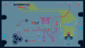
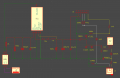
Below is the schematic and layout of the current revision. I’d like a quick check that the power filtering, decoupling, and audio/video stages are electrically sound.
Overview:
Input: 9–10 V DC barrel jack → bridge rectifier → PTC fuse + clamp diode → LM2596-5.0 V regulator.
Filtering: SS34 diode, inductor, and bulk caps per datasheet; ferrite bead isolates AV rail with 0.1 µF + 10 µF + 47 µF to GND.
Video: NPN emitter-follower buffer (2N3904 type) → 220 µF coupling cap (+ at emitter) → 75 Ω series resistor at jack → optional 220 pF to GND.
Audio: Internal and expansion audio mixed via 47 k Ω (APU) and 100 k Ω (expansion) resistors → 1 µF coupling cap → optional 100 Ω series resistor → jack ring.
Output: 3.5 mm TRS (Tip = Video, Ring = Audio, Sleeve = GND).
What I’d like feedback on:
Power/decoupling: Are my cap placements and ferrite location sufficient for isolating switcher noise?
Video path: Any signifigant issues with the transistor buffer or output coupling?
Audio mix: Does the 47 k / 100 k passive mix make sense for feeding a TV’s line-level input?
Grounding: Are there any obvious layout improvements for reducing crosstalk between the regulator and AV sections?
Thanks for any insight! I’m mostly looking for a sanity check before considering to order pcb's and components.
New face here, I’ve been developing a replacement PCB for the original Nintendo Famicom RF modulator.
It plugs into the existing 7-pin ribbon cable and replaces both the 5 V regulator and AV output stages.
The goal is a drop-in board that supplies regulated 5 V to the console and provides clean composite video + mono audio to a 3.5 mm TRS jack (wired for TRS→RCA splitters).
Below is the schematic and layout of the current revision. I’d like a quick check that the power filtering, decoupling, and audio/video stages are electrically sound.
Overview:
Input: 9–10 V DC barrel jack → bridge rectifier → PTC fuse + clamp diode → LM2596-5.0 V regulator.
Filtering: SS34 diode, inductor, and bulk caps per datasheet; ferrite bead isolates AV rail with 0.1 µF + 10 µF + 47 µF to GND.
Video: NPN emitter-follower buffer (2N3904 type) → 220 µF coupling cap (+ at emitter) → 75 Ω series resistor at jack → optional 220 pF to GND.
Audio: Internal and expansion audio mixed via 47 k Ω (APU) and 100 k Ω (expansion) resistors → 1 µF coupling cap → optional 100 Ω series resistor → jack ring.
Output: 3.5 mm TRS (Tip = Video, Ring = Audio, Sleeve = GND).
What I’d like feedback on:
Power/decoupling: Are my cap placements and ferrite location sufficient for isolating switcher noise?
Video path: Any signifigant issues with the transistor buffer or output coupling?
Audio mix: Does the 47 k / 100 k passive mix make sense for feeding a TV’s line-level input?
Grounding: Are there any obvious layout improvements for reducing crosstalk between the regulator and AV sections?
Thanks for any insight! I’m mostly looking for a sanity check before considering to order pcb's and components.
Attachments
-
 158.5 KB Views: 6
 -
 31.6 KB Views: 6


