Experience on the ESL (ECL) is needed

Thread Starter

Janis59

Joined Aug 21, 2017
1,894
Somehow I had very tiny experience with emitter coupled logics, but happened that I developed the system using an ultrafast++ comparator, where I found a brilliant AD96687 integral circuit being even better that most shameless of my dreams, so I obtained few of it, etched the pcb, mounted and only then realized that outputs are not for use a CMOS levels but ESL bipolar signal and negative levels. Damn, too small letters in the datasheet warning that this is extra special product. (http://web.pa.msu.edu/people/edmunds/HAWC/Manuals/feb_ad96685_96687_comparator.pdf)

Okay, as I was too lazy to redo anything from very beginning, I just hanged in free place the one bjt level shift cascade (common base circuit), however I applied a 1 kOhm instead of 50 Ohm recomended in datasheet. Would it be OK if I have no need for 100% of speed??

Other moment I am not sure, I used only one output not both. As it is opened emitter, I feel one hanging free may not harm the IC. Is it so??

Third moment am unsure is the latch inputs. I need no latching so I set em to +5 Volt. In the application example yet them are set to the +2V and via the 50 Ohm. May I burn something inside in my manner?? In no CMOS or TTL the straight connection to Vcc may not do ANY harm. How it is here?

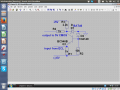
And now the problem itself: one input of operational amplifier (I mean comparator) are measure signal but other is reference voltage got from resistive divider (making by 1,5 kOhm and 1 kOhm the 1 Volt from 2,5 V stable source). Thus I was wondering why I have near 1,6V instead of 1V on that input util I realized the surplus voltage is created by IC. Cutting the connection between IC and my divider, divider part give 1V but on free hanging IC input stays 2V. So- my decision, somehow I have killed it. But I observed the most best praxes of antistatic (earhened soldering, hand chain, and pcb gnd in common conture, and I have had no any accident about input overloading. Why it burned? There is no meaning to solder it my last IC I have in the shelf before I havent understood what have been happened....
I would highly appreciate the any help in those all mess. Preliminary thanks. Your`s indeed, John.
 

Thread Starter

Janis59

Joined Aug 21, 2017
1,894
Bit detalisation of level shift cascade:
ESL output going to npn bjt (547) emitter as well as via 1 kOhm to minus 5V.The bjt base is via 10 kOhm to the same -5V and via 1n4148 to real gnd (zero volts). The collector via shottky clamp (BAT41) is to gnd, via 2,2 kOhm is to +5V and via 1 kOhm is to output wire.

Detalisation on comparator:
foot1= output, to level shifter
2=unused, hang free
3=gnd
4=gnd
5=gnd
6=minus 5 V
7=reference +2,5V
8=measured signal
9=reference +1V
10=measured signal
11=+5V
12=gnd
13=gnd
14=gnd
15=unused, hang free
16=output, to level shifter
 
Last edited:

DickCappels

Joined Aug 21, 2008
10,661
Are you using both +5V and -5.2 volt power supplies? <= thinking that not using the correct power supplies might be the cause of the offset on the input.

About the load/termination resistor:

There is a not in the datasheet that address this:
THE OUTPUTS ARE OPEN EMITTERS, REQUIRING EXTERNAL
PULL-DOWN RESISTORS. THESE RESISTORS MAY BE IN THE
RANGE OF 50-200 CONNECTED TO –2.0V, OR 200-2000 CONNECTED TO -5.2V.

The words in blue lettering at the end is my guess as to what the author intended to say.

If the output signal runs very far or is driving an edge sensitive input,I would start with 50 ohm terminations and once everything is working well, have a look with an appropriately expensive oscilloscope and see whether a mismatch is likely to be a problem.
 

Thread Starter

Janis59

Joined Aug 21, 2017
1,894
Hi! Thank You for response.

Firstly, I use +5,0 (+/- 0,1 accuracy) and -5,0 (+/- 0,1 accuracy) at the 6th feet. Ripples under 10 mV. Blocking capacitors are 10 uF `barrels` plus 47nF ceramic straight over IC (in the `second floor`).

So, except if there is large difference between 5 and -5,2 Volts (and I am rather sure both may be the same value except polarity), then power line ought not be the cause.

With the 1 kOhm or 50 Ohm, if the dynamic regime would cause the problem, then You`re right undoubtly, but defect stays at very static regime, where I simulate the levels by means of very slow change - and outputs not indicate any reaction.

Oscillo I have a type capable up to 3 GHz, but say honestly I don`t see any aim to pull it out just now, when by means of much slower 50 MHz I see everything stays totally calm.

Anyway, IC is got desoldered just now (with rather minor deglued patches of pcb), so nearest days will show what happens with the last IC out of the box.
 

Thread Starter

Janis59

Joined Aug 21, 2017
1,894
Ouch, what`s about the sequence of PS !!!??
If ATX for PC makes a pon sequence wrongly, then harm is near imminent.
Probably that is the similar reason in this case??
As I apply the two separate phone charger units with add-on LDO, and both are plugged without of thought about sequence.
Does the sequence has the place here?
Do the ECL may burn if few seconds have left with just one (plus or minus) power, whilst other is unplugged?
 

RichardO

Joined May 4, 2013
2,270
I am having a hard time visualizing your level shifting circuit.

Can you post a sketch of the circuit? I will simulate it in LTspice.
 

Thread Starter

Janis59

Joined Aug 21, 2017
1,894
RE:RichardO
<<Can you post a sketch of the circuit>>
Here is the level shift part, connected to 16th feet and identical other to 1st feet.
But I wonder if it is possible to crush the operational amplifier input by wrong load to operational-steered ECL output.
The meaning of all circuit together: when measure point voltage on capacitor is less than 1,0V then flip-flop is switched off, and when it is larger than 2,5V then flip-flop is switched on. The flip-flop is made on basis of 74AS02D - just the cross-linked two cells.
Demands for speed is set by work frequency 6 MHz with frontier better than 1% of cycle-time, thus risetime or falltime must be better than 600 MHz (~4 nsec). Therefore 1 ns advertisement for AD96687 looked rather fine.
 

Attachments

Thread Starter

Janis59

Joined Aug 21, 2017
1,894
By the way, please dont miss to say a word do the ECL IC is sensitive about time-shift in power on, between positive and negative. Today I think, it may be the key to my riddle (if there is sensitivity), as I switch positive one by one hand and other negative by second hand.
 

RichardO

Joined May 4, 2013
2,270
By the way, please dont miss to say a word do the ECL IC is sensitive about time-shift in power on, between positive and negative. Today I think, it may be the key to my riddle (if there is sensitivity), as I switch positive one by one hand and other negative by second hand.
I have never damaged an ECL comparator and have not sequenced the power. I have always used power supply supplies limited to an amp or so, however.
 

RichardO

Joined May 4, 2013
2,270
By the way, please dont miss to say a word do the ECL IC is sensitive about time-shift in power on, between positive and negative. Today I think, it may be the key to my riddle (if there is sensitivity), as I switch positive one by one hand and other negative by second hand.
To be safe, you can put some high current Schottky diodes across the power supplies to clamp the voltages.
 

Thread Starter

Janis59

Joined Aug 21, 2017
1,894
Aha, then sequence has no role, like it is at normal operational amplifier.
One prime suspect then is shoot.
Those PS has about 0,4A maximum.

OKay, for a while I`m going to sleep, its near midnight. Tomorrow morning I shall read Your thoughts with an impatience.
 

Thread Starter

Janis59

Joined Aug 21, 2017
1,894
Thanks, it looks quite nice however the going off from common base means I need a bjt with no less than 600*100=60 GHz F(T). At least the 40 GHz I know where to obtain, but it complicates all the thing, as so much count of components are nowhere to squeeze into already compact pcb.
Anyway, Your circuit I shall put in my ideas folder for use the next time I shall meet the ECL. Generally I like it. Thanks.
 

RichardO

Joined May 4, 2013
2,270
Did you get the '687 working?

I occurred to me that you might not have the enable signals for the latch connected correctly. They have to be complementary ECL levels. The latch signal must be a logic high to allow the comparator output to change -- that is, to follow the input.

I have attached a slightly different data sheet for the '687 comparator. See the general description in the attached data sheet.
 

Attachments

RichardO

Joined May 4, 2013
2,270
Thanks, it looks quite nice however the going off from common base means I need a bjt with no less than 600*100=60 GHz F(T). At least the 40 GHz I know where to obtain, but it complicates all the thing, as so much count of components are nowhere to squeeze into already compact pcb.
Anyway, Your circuit I shall put in my ideas folder for use the next time I shall meet the ECL. Generally I like it. Thanks.
Yeah, it might very well be easier to just use the right part even if you have to hand wire it onto your prototype PCB. Linear Tech (and others) have some really fast CMOS compatible comparators. The LT1720 comes to mind.
 

Thread Starter

Janis59

Joined Aug 21, 2017
1,894
Thanks for suggestion.
Its bit slow, but probably tolerable.
The student of whom I am his graduation work leader still haven’t soldered the last 1 nS IC I have, so I haven’t yet ready to tell of success or vice versa, but if anything will be going wrong with that, its absolutely sure that 1720 will be the next to experiment.
I may only regret I not choose it from the very beginning.
 

Thread Starter

Janis59

Joined Aug 21, 2017
1,894
Hi!
1) Today I had time to build a Spice model for level shift circuit, those kind of one bjt with common base. In the model it works brilliantly.
2) At last I figured ut what was the reason why IC was burnt. Its laughfully prost. The LATCH and NON-LACH I switched where written logic 1 means to +5 and where written logic zero - to gnd what is ) Volts. Wrong, wrong, wrong. That was meant to connect to the ECL logic zero and ECL logic one..... Or other words minus 1,1 and minus 1,5 Volts.
So, there is no doubt why switching the +5 instead of minus 1,1 the whole input chains are totally demolished with burnt ash-holes. The solution I applied was three resistors in the series, deepest from -5V was 24kOhm, upper it 2,7k and last - most upper to the gnd 7,5k. From deepest (nearest to -5V) connection point of resistors happens -1,5V or logic low, what is latch non-enable and from nearest to gnd connection point of resistors happens logic high -1,1V or signal for input latch enable.
Thus, the problem may count solved for a while.
 

RichardO

Joined May 4, 2013
2,270
Hi!
1) Today I had time to build a Spice model for level shift circuit, those kind of one bjt with common base. In the model it works brilliantly.
2) At last I figured ut what was the reason why IC was burnt. Its laughfully prost. The LATCH and NON-LACH I switched where written logic 1 means to +5 and where written logic zero - to gnd what is ) Volts. Wrong, wrong, wrong. That was meant to connect to the ECL logic zero and ECL logic one..... Or other words minus 1,1 and minus 1,5 Volts.
So, there is no doubt why switching the +5 instead of minus 1,1 the whole input chains are totally demolished with burnt ash-holes. The solution I applied was three resistors in the series, deepest from -5V was 24kOhm, upper it 2,7k and last - most upper to the gnd 7,5k. From deepest (nearest to -5V) connection point of resistors happens -1,5V or logic low, what is latch non-enable and from nearest to gnd connection point of resistors happens logic high -1,1V or signal for input latch enable.
Thus, the problem may count solved for a while.
Good to hear that things are progressing. :D

Oh, those poor innocent comparators. ;) I can see how your error happened. You were thinking CMOS, not ECL.

I normally think of ECL high being 0.9 volts and ECL low being -1.8 volts. Your -1.1V and -1.5V will likely work, though.
 
Top