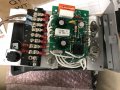
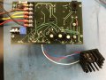
i rose the TF power / replaced some transistors - - - it still shows a poor regulation / so i experimented with few changes . . .
this is a random experiment -- don't adapt anything "just incase" (( the MB stands for More Bower ))
#35 -- hints that it is a precision target application - - - while the simulators give you usually a general overview of the circuit interrelations logic = it suggest how (not by how much) to adjust component parameters(with the simulators there is always tendency to go too idealistic -- precise tuning the resistor values that most definitely won't match those on the real circuit ...) /// besides the BUL6823 used has the hFE 12...22 (although it tolerates 400V collector voltage) it goes far from design you are working on
your design is principally done (well/) out of the book -- they just untied the Load GND from the regulator 1 ...
________________
did and a Gizmoless sim. that shows that the transformer (i came up with) needs to be more powerful = the demanded power starts to exceed that provided just about at 55V OUTP (e.g if there were a SC protection as in your circuit and/or a shunting zener -- it wouldn't work/regulate at all) (another thing not tested is high power draw at low output voltages = at high power at regulator-switch transistor) - there is no limitting resistor needed for a darlington switch at moderate output currents (it should be re- verified for max. (near SC(short circuit)) currents) etc. etc. View attachment 188235+ about the "AND" View attachment 188245View attachment 188246View attachment 188247View attachment 188248
Can you tell me what the C11 and C4 capacitors are doing in your simulation? Are they showing possible oscillation? Or are they added to try and reduce output transistor heating? I can't easily follow what you were doing in layman's terms.
An old engineer told me recently that because of the magnet in the design to engage, not springs, the magnet when it heats up loses efficiency, so voltage needs to change as the coil heats up, to accomdate the magnet. So maybe the inefficiency of design is designed that way?
they illustrate the possible behaviour of the (power) "switch" of the emitter load voltage regulator
PS! -- yes, as the primary function they do not affect the thermal profile of the Q4 much and are provided to show how to keep Q4 from oscillating while such is required also the simulations illustrate what i mentioned in #30
C11 acts as "low pass element" to attached load
C11 also acts as voltage integrator
↑both of which are trivial and obvious↑
so the C4 is a different beast -- basically it softens the waveform on Q4 as ::
• if there is variation in load
. . the C4 passes the sharp *transition fronts 1-st (acting as AC shunt)
. . only then the base of Q4 gets affected by* (it also conditionally compensates the Q4's possible inability to provide High Power fast)
• if the power demand of the OUTP (load) approaches the INP (supply) capabilities , and also at- and near the OUTP's short circuit condition
/// ups! i passed a bug -- coz at SC oscillation it makes the ON share longer and likely (most cases) won't cancel the "switching"
. . the Q4 may start switching/oscillating ← in this condition the regulation may dramatically differ from that of the non-oscillationg/switching one
. . so if you do not want to regulate the OUTP for the switching Q4 also THEN it is better to keep it from switching
PS+ ! -- as the secondary function the C4 is one possible measure to keep (the regulating el.) Q4 at "continuous" mode (if it were not) and that in turn may keep the temperature down (in case if the Q4 was switching and that mode was not desired handled and if it was the cause of the heat-up of regulating element . . . )
. The senior engineer likely can point out all the special features built in to your "brake drive supply"
_______________
. . . sometimes the seemingly simple circuits have "coded in" complex functionality
← you will be able to see such when you design 100-s of regulators for the different purposes
and after getting this experience
when you then need a simple regulator
you only "include"/provide the *functions for given margins (obviously trading between the precision/"efficiency" of each*) . . . ←
← . . . however that (in turn) is very lucky coincidence if you know how to enable things simply -- or then it's an exhausting lot of work reaching the simplicity of the design for specific requirements
 Facebook
 Google
 GitHub
 Linkedin
") ))
))