@ #1
you might try to introduce a cople of resistors
1-st to Q1 collector (in order to reduce momentarily current through it , and lower it's probable V.CE . . . also enabling more current through Q2 as it reduces the neg. collector feedback of Q2 -- is precision tuning)
2-nd from the base of Q2 to GND or to it's emitter (to make it base voltage more stable)
perhaps a cap (100pF up to 100µF) across 2N3055 C-E (← but this is relational design element that may need more mod.-s to the circuit -- while it has any effect to your problem at first place - must be verified that the problem with 2N3055 is it's oscillating with inductive load - must be verified that shunting the power switch has supressing effect on such ← may require to redesign the circuit and at the input side to 2N3055 ... )
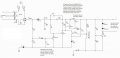
Here is the actual full circuit, attached. I have tried doubling output transistors (both of the Darlington set up- 4 transistors). I have also tried 2 Mosfets (R5- 100 ohm base emitter resistor removed and Q2 removed- base emitter jumped) with 1 ohm source (what would be emitter) resistors tied to output (temps were a little uneven 20F between), but this worked. If I can use the 2 fets I could use one heatsink, with fet on each side of the heatsink. I suppose I could also replace the other 2N6308 in the negative output lead with a fet, just don't know the resistor value changes to do that.
If, in the power supply rectifier section, you remove the ground connection from the negative terminal of the bridge rectifier and instead connect it to the transformer at terminals 6 and 7, which is functionally the secondary center point, that might bring the input voltage down to a level that would give very little heating of the transistors. You might need to use a higher value of capacitance at the filter, C3.
And right now I am wondering how you get any voltage out with C1 in series with the DC line. Are you certain it is in the right place? It does not look right.
? is the Q4 emitter connected as shown on your figure or is there something missing/not-so . . . or then it's Q3 , D5
- - - -
if the connections are as shown you want to AC shunt the Q5 with large capacitor . . . and maybe some more schematic adjustments
- - - -
perhaps you write next to each block of your schematic what it was meant to do/handle
If, in the power supply rectifier section, you remove the ground connection from the negative terminal of the bridge rectifier and instead connect it to the transformer at terminals 6 and 7, which is functionally the secondary center point, that might bring the input voltage down to a level that would give very little heating of the transistors. You might need to use a higher value of capacitance at the filter, C3.
And right now I am wondering how you get any voltage out with C1 in series with the DC line. Are you certain it is in the right place? It does not look right.
There's a switch across C1 (or jumper), not shown. C2 is the power supply filter. C3 was added when some oscillation was found Q1 base to emitter, but removed when it was found not doing anything. I need the adjustability to 80VDC, this is for different coils that need specific voltages applied, staying the same voltage with AC line change. So lowering the AC volts is not an option.
@ #1
you might try to introduce a cople of resistors
1-st to Q1 collector (in order to reduce momentarily current through it , and lower it's probable V.CE . . . also enabling more current through Q2 as it reduces the neg. collector feedback of Q2 -- is precision tuning)
2-nd from the base of Q2 to GND or to it's emitter (to make it base voltage more stable)
perhaps a cap (100pF up to 100µF) across 2N3055 C-E (← but this is relational design element that may need more mod.-s to the circuit -- while it has any effect to your problem at first place - must be verified that the problem with 2N3055 is it's oscillating with inductive load - must be verified that shunting the power switch has suppressing effect on such ← may require to redesign the circuit and at the input side to 2N3055 ... )
Thanks,
I can experiment with resistors on Q1 collector and Q2 base. I can try a couple capacitors also C to E. There was oscillation Q1 base to emitter, once C3 removed or lowered value, oscillation went away.
? is the Q4 emitter connected as shown on your figure or is there something missing/not-so . . . or then it's Q3 , D5
- - - -
if the connections are as shown you want to AC shunt the Q5 with large capacitor . . . and maybe some more schematic adjustments
- - - -
perhaps you write next to each block of your schematic what it was meant to do/handle
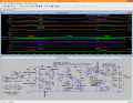
A simple way to reduce the load on your regulator, and still have the higher voltage available when needed, is to place a series resistor between the filter and the regulator with a bypass switch across it.
This assumes the regulator has decent line regulation to work.
The resistor will bear some of the load, but the overall wattage will not be reduced.
You can use any number of resistors and bypass switches.
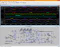
more likely it's required in parallel with Q5 CE junction OR in parallel with Q5 and R12 OR 2 caps - 1 for each of Q5 and R12
less likely (or if there was no Q5 or if the Q5 is firmly conducting = acting as a resistor) and if there is a squarewave OUTP at Q1 emitter
e.g. if the Q1 is oscillating (due inductive load feedback trough it's emitter) and if the 47pF from Q2 base to Q2 collector wont fix that issue
then the next thing to try would be voluntary cap from Q1 Collector to its Emitter + That cap must see the filter Cap over the OUTPUT (55V node 6 node 5) ← and then much likely the Q5-R12 still need the parallel Cap(s) to complete "that AC-path"
↑↑ there is nothing certain in that ↑↑ -- must be tested out - by error trial
the first rule is to build the supply without any filter caps -- then if it starts oscillation -- you follow "patching the leaks" 1 by 1
i missed the simple fact of 80 to 15 V output e.g. 75*√2 - 15 = 91V on Q1 incase of 15V output
- - - - so you could utilize the Q5 in series with Q1 to div that by 2
Right now the Q5 acts as Collector Load Regulator..
(usually used in switching regulators to enable faster switching times and higher loads)
(or for Short Circuit Proofing -- as is and right now).. and drops 1.5V
you can intercept the TF from high side and regulate from there ←← but this rises the difficulty level of your design by order of 2(as from 1 to 3)
option2 is to put a "tracking pre-regulator" before the one already present that keeps the 6V headroom for it ... (i've done ← such to cut down 50Hz ripple -- not to balance thermal budget -- and to enable larger name- lower voltage value filter caps before last stg. ...)
If you put a resistor in each emitter of the parallel transistors it will help to balance the current between them. The resistors should drop about 0.3V at the current which will be flowing in each transistor.
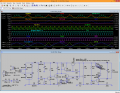
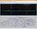
i explored the properties of this thing
the simulations are messy but they ident. potential issues (at least for components used in simulation = i don't have your models)
poor regulation
the darlington can't be made work alike likely the reg. cuts off too much drive voltage (← needs retouch - the design)
the Q5 prevents 300mA at 55V
the circuit (( to the left of std. ref. (3V zener + NPN) ))
depends on INP voltage (this is not good at all weather)
. . . more -- i don't quite understand the exact purpose of everything there
. . . so i can't tune it up against anything
. . . i just assumed "normal" linear reg. and tested the basic regulation as best i could guess the function of grid elements..
didn't want to make the transformer more powerful as that (but it might be)
the numbers indicate rising timeline of changes (not that any should be preferred to others)
-- i didn't work it out , so someone might ...
+ a basic simple quick compile for fixed 55V output (just to see misc control currents and voltage points) not-simplified/optimized fully tested ...
next to check is constant 300mA draw at 55V -- if C8 drains -- the supply rings in
? perhaps the voltage doubler fixes this ← such is all fun where some tiny requirement makes the design options to contradict . . . because doubler re-introduces the thermal (→update→) + Static Load Test + "fitting in" without the voltage doubler (the opts are avail but i had to use more trackable layout)
One other option, if the supply must be able to cover a very wide range of output voltages, is to copy the method used in one of the B&K power supplies. As the voltage range was changed there were switches to change the connection point on the transformer. This method improves efficiency a great deal, since the voltage drop across the regulator can be much less, no matter what the voltage setting is.
This is the only simple way to avoid the poor efficiency and heat generation using a linear voltage or current regulator system.
What has never been adequately described is the actual application of this system. It may be that a regulated power supply is not the best device for whatever is being done with an inductive load, whatever inductance that has. 55 volts is not a standard voltage, and at 300mA is a moderate amount of power. And the fast cutoff requirement is a bit of a puzzle to me.
The inductive load is a magnetically engaged brake. The voltage must be at 52 to 58 volts to release the armature. But different size brakes will need different voltage ranges to do this. The fast shut off has something to do with allowing no flux to prevent the magnet part of the brake from re-engaging. I am not sure of this, I am helping an engineer redesign an old control that was hand wired- transistors mounted to a metal plate, now components are on 1 pcb not hand wiring, but way hotter running, because no plate. The idea was to eliminate the hand wiring.
The inductive load is a magnetically engaged brake. The voltage must be at 52 to 58 volts to release the armature. But different size brakes will need different voltage ranges to do this. The fast shut off has something to do with allowing no flux to prevent the magnet part of the brake from re-engaging. I am not sure of this, I am helping an engineer redesign an old control that was hand wired- transistors mounted to a metal plate, now components are on 1 pcb not hand wiring, but way hotter running, because no plate. The idea was to eliminate the hand wiring.
The attached Magnet Brake temp testing was done with the old hand wired control. As temp goes up coil current goes down, so voltage must be somewhat stable. Some coil applications the supply must be constant current, but I'm not sure what this design was meant to be, looks like a standard DC supply keeping voltage constant. Thanks ci139 for the spice simulations, I have heard of this type of modeling, looks interesting and helpful.
Thank you for the explanation, it helps a lot in making sense of the requirements. One comment about the fast shutoff as a means of preventing re-engaging is that in an application that demanded a quick release of a magnetized part, the solution was a brief pulse of the opposite polarity. That worked well in one application. My guess is that the brake is spring released rather then just plain allowed to separate.
One common reality of magnetic motion is that the force increases as the air-gap gets smaller. So probably the current needed to hold the brake engaged to withstand a given torque load will drop as the brake engages. And of course, with a constant voltage the current will drop as the windings heat and the resistance rises. The way around that is to use a constant current regulator, which gets a bit complicated with an inductive load.
Unfortunately there is no simple way of reducing the dissipated power in the driver circuit if you have a constant voltage from a transformer. Going to a switching mode constant current regulator would work, and cut the dissipation quite a bit, but it is not simple. It is entirely possible, just not simple.
#35 -- hints that it is a precision target application - - - while the simulators give you usually a general overview of the circuit interrelations logic = it suggest how (not by how much) to adjust component parameters(with the simulators there is always tendency to go too idealistic -- precise tuning the resistor values that most definitely won't match those on the real circuit ...) /// besides the BUL6823 used has the hFE 12...22 (although it tolerates 400V collector voltage) it goes far from design you are working on
your design is principally done (well/) out of the book -- they just untied the Load GND from the regulator 1 ...
________________
did and a Gizmoless sim. that shows that the transformer (i came up with) needs to be more powerful = the demanded power starts to exceed that provided just about at 55V OUTP (e.g if there were a SC protection as in your circuit and/or a shunting zener -- it wouldn't work/regulate at all) (another thing not tested is high power draw at low output voltages = at high power at regulator-switch transistor) - there is no limitting resistor needed for a darlington switch at moderate output currents (it should be re- verified for max. (near SC(short circuit)) currents) etc. etc. + about the "AND"
how does the PCB mount disable using the old heat sinks ("metal plates") as they were
((the mosfet acts as a darlington and is more prone to oscillations usually requires a small resistor to it's source to damp down too fast responce)) those zeners would go FW conducting FlyBacks at "power cut" 266Ω 210mA inductor has the inductivity of around 5H
((but the experiments i condacted went loss when the Seagate HDD's BOOT sector wore out -- so it's a far estimate from my poor memory about not daily used data)) Quick Falstad check up ... 100ms to get to full power
 Facebook
 Google
 GitHub
 Linkedin