Eagle - One big shematic splitted in few PCB boards

Thread Starter

Josip Bajo

Joined May 15, 2017
5
Hello everyone,

any help is appreciated...

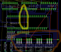
I am working in Eagle and having a one big shematic (consists with lots of elemts and around 40 RGB LED).

Things is those RGB led, are having different location around 1 meter; they are spreaded differently, so it is really not practical to have one board. What I want to do, is to have a main board with microcontroller and other necessities for cirucits; and on other three boards have only my RGB led in group of 5 to 10.

I have shematic; and now working on .brd file. I succeed to do my main part with microcontroler etc...

But now trying to put my RGB led in different groups and connect it to the main board.
I am not exactly sure which connectors to use, and the air wires or wires that are still between my two boards that I imagine to make; what with those wires, to layer them to connector or what?

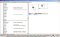
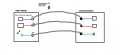
I uploaded my "idea" if it is possible in any way.

Down is the main boards (the brain), and the other boards are just LED; i want special boards for LED, because for my projects in general, they need to be on different sides.

So is it possible to somehow connect these 4 boards in between? My main concern is how to get rid of those yellow air wires (with layers?) and how to connect boards between themselve?


thank you :)
 

Attachments

The schematic usually just contains all of the parts on a single board.

If you want parts on a different board, create a separate schematic containing only those parts.

If you are putting everything on the same schematic/layout for manufacturing reasons, disconnect all connections for parts on different boards. Add connectors or vias instead of direct connections.
 

SLK001

Joined Nov 29, 2011
1,549
+1 on creating 1 schematic -1 board. You need to add a connector element (even if it is just a wire soldered into a hole) on boards that need them. It's not difficult, you just need to keep things straight in your head.
 

Thread Starter

Josip Bajo

Joined May 15, 2017
5
Thank guys! :D
Ok. Then I will put holes on my board.

1. Can I use the those holes that are offered in Draw tab in Eagle under Holes. I've attached a picture below.
What I am planning with those holes is t put them on boards, and then solder a wires on those holes, and that is how I am planning to connect signals between my multiples boards? Should this work as an idea?

Other idea is to use a flat cable connector to connect the boards. Something like this:
http://www.wcon.com/uploads/www.wco.../94df1958029b8c356bc70f139ffcb368_430x430.jpg
https://cdn.usdigital.com/assets/images/galleries/ca-c10-f-c10_0.jpg

But things is, I get pretty anxious when I search for the proper connector in Eagle library, what to find, and what will fit. That is why I am also thinking about holes... :O

I have whole idea of my sheme and project, but it is only this connection in between; so I am really grateful for any more advice which solution is better.

2. And just one more question, for those who know Eagle.
If Eagle autorute can not connect all elements on one board with only bottom (blue layer) then it is not possible. I am trying to finish my boards only with bottom (blue) layer, because it is easier to solder.
Autorute can't do it with only bottom layer, and I am struggling also; so it is not possible and I should split boards or try harder to connect everything?


Thank you guys for posts above and advices! :)
 

Attachments

The connection as SLK001 has shown is a good method. It lets you connect as many wires as needed.

If you look for a connector, look at the number of pins and the distance between pins. It is often a good idea to print out the footprint and physically place the part on it to be sure it is the correct configuration. Not exact but often enough.

Concerning an unroutable design, you can put wire jumpers in as a component, on the schematic and/or pcb to help jump over some of the other PCB wires.
 

Thread Starter

Josip Bajo

Joined May 15, 2017
5
Guys you are my saviours, of time and nerves! :)

Thank you so much for you help.

I finally have final strategy and everything is clear ( I hope so).

Just to resume, if this sounds good to you:

1. For overlapping lines in bottom layer, I will use this strategy of jumper wires.
I've found two options to create them. To add a jumper in shematics, and then connect them while creating .brd file.
Or another options use a top (red layer) for these lines that I can not connect. When I connect those with top layer, vias are automatically made. And I have a jumper now.
And then, when I print my boards, I just tell it to not print top (red layer). But vias will stay on board. Then If I understood right, I need to with marker conenct those vias? Is this right or misunderstood it?

I have uploaded Picture 1; how I connected mine "jumper wires". Is this ok? I think yellow circle is ok; when I print it, I should just connect vias with the marker or?

But the brown circle that I marked, I am suspicious, I think they also must not overlap?


2. And second things, I realized for connector between two boards.
When I need to connect my boards, either I will drill the holes, to solder s wire that will connect two wires from different boards.
Or I will use some connector with pins (I think this is smoother solution). In that case, one pin is connecting two wires from different boards?
I added a picture 2, as an sketched idea of how would I do this.

I just need confirmation if I got this right?

Thank you very much for advices and knowledge for sharing with.
 

Attachments

Not a fan of how you routed things on the red layer. The jumpers are often just the size of a resistor as they are in you design. The would be labeled as zero ohm resistors. This keeps the design neat, whereas your jumpers are running all over the place.

If you are going to put them on the PCB, put them on in such a way that the DRC, design rule check, capability of the tool still functions. The DRC check is there to ensure the board follows the trace width and distance from other track rules. It is always nice to see no errors when the check is run.

Also, if you make a single sided board, the vias will not be connected through the board. There won't be pads on the top layer to solder to. This may be o.k. but make sure you have access to all of the jumper vias where you want them.
 

Thread Starter

Josip Bajo

Joined May 15, 2017
5
Also, if you make a single sided board, the vias will not be connected through the board. There won't be pads on the top layer to solder to. This may be o.k. but make sure you have access to all of the jumper vias where you want them.
I did not catch this part. I am planning a single sided board, so not soldering on top layer.
I am planning just to solder components and with his jumpers connection is going to work. Or I got it all wrong? :O
Because, as I mentiond up, after making jumpers, when I print my boards, I should connect vias with marker? and should this work? Or this process is working differently?
 
Not sure what you mean by connecting the vias with a marker.

I think it is good to at least place the traces on the board in a fashion that allows the error checking to function properly. It can also show exactly how you want to place your jumpers on the board.
 
Top