Different IR2184 behavior when driven from Arduino D9 vs D10

Thread Starter

eliegeob

Joined Oct 6, 2025
27
Hello,

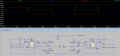
I’m working on a project where an Arduino generates a 40 kHz PWM signal to drive a piezo transducer through a full-bridge (H-bridge). In LTspice, the H-bridge + IR2184 driver stage behaves as expected.

In hardware, I generate complementary PWM on Arduino Uno pins D9 (OC1A) and D10 (OC1B) using Timer1 fast PWM (mode 14, TOP=ICR1):

  • f ≈ 40 kHz (ICR1 = 399 @ 16 MHz, prescaler = 1)
  • 50% duty (OCR1A = OCR1B = 200)
  • D9 non-inverting, D10 inverting (COM1B0 set)
So logically: D9 = PWM, D10 = inverse(PWM).

Problem: When connecting these outputs to the IR2184 input(s), the waveforms look different depending on whether I use D9 or D10. In particular, the driver output stage looks “correct” only when driven from D10, while driving from D9 produces ringing / an unexpected waveform after the IR2184. This is confusing because the Arduino outputs are complementary and come from the same timer.

What I’ve checked / observed:

  • Arduino 5V rail is about 4.64 V (USB powered), so GPIO high is ~4.6 V max.
  • Both channels are measured with the same scope/probe, common ground.
  • The effect becomes much more visible once the IR2184 input is connected (compared to probing the Arduino pins unloaded).
  • Scope captures show ringing/overshoot on one path more than the other.

Question:
Could this be explained by pin driver differences (OC1A vs OC1B), input capacitance of the IR2184, breadboard/jumper inductance, and/or probe ground inductance causing different ringing depending on the pin? If so, is the standard fix to add a small series resistor (e.g. 47–100 Ω) at each Arduino output right at the MCU pin to damp the edge and reduce ringing?

I’ve attached:

  • LTspice schematic
  • Arduino timer code
  • Scope screenshots / comparison table

Any insight into why the driver outputs differ depending on D9 vs D10 (and how to make them behave consistently) would be appreciated.

Thanks!
 

Attachments

AVR output drivers are not totally identical. Each GPIO pin has its own output transistor pair. Rise/fall times, output impedance, and internal routing vary slightly per pin. These differences are negligible when driving LEDs but visible at 40 kHz with fast edges into a capacitive load. Adding small series resistors can solve this problem. You can start with 47 ohm and see if it solves the problem. You can also test with 100 ohms and compare which performs better.
 

Thread Starter

eliegeob

Joined Oct 6, 2025
27
AVR output drivers are not totally identical. Each GPIO pin has its own output transistor pair. Rise/fall times, output impedance, and internal routing vary slightly per pin. These differences are negligible when driving LEDs but visible at 40 kHz with fast edges into a capacitive load. Adding small series resistors can solve this problem. You can start with 47 ohm and see if it solves the problem. You can also test with 100 ohms and compare which performs better.
hello, so you mean if i add a 68 ohm in eries from the arduino pin to the input of the mosfet driver, it should work?
thank you.
 
hello, so you mean if i add a 68 ohm in eries from the arduino pin to the input of the mosfet driver, it should work?
thank you.
Yes. This is what I mean.
Arduino D9 - 68ohm -HIN (IR2184)
Arduino D10 - 68ohm-LIN (IR2184)
The series resistor increases the source impedance of the Arduino pin. This damps the LC resonance formed by the wiring inductance and the IR2184 input capacitance. It reduces overshoot, ringing, and false triggering at the IR2184 input.
At 40 kHz, the slight slowing of the edges is negligible, the driver still sees a clean digital signal.
 

Thread Starter

eliegeob

Joined Oct 6, 2025
27
Yes. This is what I mean.
Arduino D9 - 68ohm -HIN (IR2184)
Arduino D10 - 68ohm-LIN (IR2184)
The series resistor increases the source impedance of the Arduino pin. This damps the LC resonance formed by the wiring inductance and the IR2184 input capacitance. It reduces overshoot, ringing, and false triggering at the IR2184 input.
At 40 kHz, the slight slowing of the edges is negligible, the driver still sees a clean digital signal.
Hello,
alright this makes sense, i hope it will work. so if i understand correctly this resistance will make the pins behave almost identically by damping the LC resonance.
Thank you in advance:)
 

panic mode

Joined Oct 10, 2011
4,947
where did all capacitors go or am i missing something. there was supposed to be at least three per IR2184.
1770818815364.png

your sim shows 100nF - how did you determine value of capacitors? there is a formula in there and if you are just going by examples, 100nF is the absolute lowest that i have seen. often shown values are 10..20+ times larger. breadboard capacitance is much too low for this (some 20pF)

1770819332796.png
 
Last edited:

Thread Starter

eliegeob

Joined Oct 6, 2025
27
where did all capacitors go or am i missing something. there was supposed to be at least three per IR2184.
View attachment 363352

your sim shows 100nF - how did you determine value of capacitors? there is a formula in there and if you are just going by examples, 100nF is the absolute lowest that i have seen. often shown values are 10..20+ times larger. breadboard capacitance is much too low for this (some 20pF)

View attachment 363353
Hello,
there is one capacitor going from pin 6 to pin 8 on the mosfet driver. and i only used one capacitor, why would i need 3? in the diagram you sent it is for the ir21844s (with dead time) in my case i dont have this, i am using the ir2184. and i chose the capacitance based on the total gate charge of the mosfet which is 70 nC and the Supply current drawn from VB when HO is high is 150 uA, with Ton = 12.5us, so i got the driver charger consumption and the mosfet gate charge and i got 103nf. bootstrap capacitor = total required charge/allowed voltage drop.
In any case of confusion please let me know:)
 

panic mode

Joined Oct 10, 2011
4,947
fine, for IR2184 it is two of them:
1770830299637.png
i still do not see that capacitor on your breadboard or capacitor across Vcc and COM. and there is a second chip for the other pair of transistors. also no capacitors there...
 

Thread Starter

eliegeob

Joined Oct 6, 2025
27
fine, for IR2184 it is two of them:
View attachment 363357
i still do not see that capacitor on your breadboard or capacitor across Vcc and COM. and there is a second chip for the other pair of transistors. also no capacitors there...
the capacitor between Vb and Vs is there it has the beige color like this.1770832769615.png1770832742287.png
and for the capacitor between com and VCC i simply didnt see the point of putting a capacitor there. could you explain to me why would i put a capacitor there? and the capacitors on the transistors side as well?
thank you.
 

panic mode

Joined Oct 10, 2011
4,947
aha... well camouflaged behind those wires and blending with breadboard.. :D
about supply side cap:
1. it is in the datasheet... that alone means do not ignore it.
2. it is a well established practice to put bypass/decoupling capacitor across each and every IC - close to ICs power terminals - specially for digital ICs, switching circuits and drivers. usual values are 0.01 - 1.0uF with 100nF being most common.
3. one may be tempted to skip them (or use fewer) when circuit is on a PCB. do so with caution. but when using protoboard, and long wires like your circuit, you would want to use it (and double it) to mitigate noise, ringing etc.

you can read about it here or here.

and check typical TTL board - notice caps next to each IC:
https://upload.wikimedia.org/wikipedia/commons/a/a5/Cromemco_16KZ_S-100_Board.jpg
 
Last edited:
the capacitor between Vb and Vs is there it has the beige color like this.View attachment 363359View attachment 363358
and for the capacitor between com and VCC i simply didnt see the point of putting a capacitor there. could you explain to me why would i put a capacitor there? and the capacitors on the transistors side as well?
thank you.
Oh. I did not see this picture earlier. Actually there are lots of sources of noise in such breadboard circuits. Loose connections, low quality jumper wires are among those. If adding the series resistor solves the problem, very good. If not, I think it's better to prototype a PCB.
 

Thread Starter

eliegeob

Joined Oct 6, 2025
27
Oh. I did not see this picture earlier. Actually there are lots of sources of noise in such breadboard circuits. Loose connections, low quality jumper wires are among those. If adding the series resistor solves the problem, very good. If not, I think it's better to prototype a PCB.
Hello,
thank you for your advice but turns out that the D9 from the arduino microcontroller was broken and probably because i didnt have the capacitors like you mentioned. but i also have an additional question regarding the signal on the oscilloscope. i am trying to measure the signal at the receiver of a piezo given that the sender is the load of this H-bridge, but the signal looks really bad in a way that i see band of lines instead of just a clear or near clean signal. the receiver terminal pins are connected to the oscilloscope probe. do you think i should connect one of the terminals of the receiver to the same ground as the piezo sender?
 
Yes, connect the receiver ground to the sender ground. Without a common ground, the scope shows floating voltages.
This causes bands or fuzzy lines on the display. Piezos have high impedance, making signals very sensitive. Use the shortest probe ground to reduce noise. Active probes help if signal amplitude is small. Proper grounding cleans the waveform and shows real 40 kHz signals.
 

Thread Starter

eliegeob

Joined Oct 6, 2025
27
i did that and this is what i am still getting, purple is the signal at the receiver . what i am indeed noticing is that
when the sender and receiver move toward each other, the received frequency increases (wavefronts are compressed).
when they move away from each other, the received frequency decreases (wavefronts are stretched). but it is just not really clear here and i want it to be clear since i want to measure the phase shift between this receiver and another receiver.1770980494276.png
 

drjohsmith

Joined Dec 13, 2021
1,584
i did that and this is what i am still getting, purple is the signal at the receiver . what i am indeed noticing is that
when the sender and receiver move toward each other, the received frequency increases (wavefronts are compressed).
when they move away from each other, the received frequency decreases (wavefronts are stretched). but it is just not really clear here and i want it to be clear since i want to measure the phase shift between this receiver and another receiver.View attachment 363396
This is a fast edge signal.
You need very good decoupling on the breadboard to make that work..
I'm guessing your using the long earth clip on the scope probe ? Try using the short spring thing that clips around the scope probe end , connected close to the earth of the driver.
 

Thread Starter

eliegeob

Joined Oct 6, 2025
27
This is a fast edge signal.
You need very good decoupling on the breadboard to make that work..
I'm guessing your using the long earth clip on the scope probe ? Try using the short spring thing that clips around the scope probe end , connected close to the earth of the driver.
for decoupling i use 100nF capacitors on the IC. and i used the scope probe with a spring attached to the gnd and the crocodile scope probe i connected it on on terminal of the piezo sender and i got this. yellow is the sender and purple is the receiver. 1770990442934.png
 

drjohsmith

Joined Dec 13, 2021
1,584
for decoupling i use 100nF capacitors on the IC. and i used the scope probe with a spring attached to the gnd and the crocodile scope probe i connected it on on terminal of the piezo sender and i got this. yellow is the sender and purple is the receiver. View attachment 363399
On a probe , you only connect the crocodile clip or the small spring clip.
You need to use the small spring clip on both probes.
It could just be your board , can you share picture of you proving the signals please.
 
Top