 Facebook
 Google
 GitHub
 Linkedin
Dear friends. I have made AC analysis for a simple 2N5486 based common source amplifier. The circuit is below:

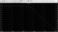
My LTspice AC analysis of the circuit delivered the following result:

I was surprised to see magnitude plot having the magnitude increasing with frequency increase. I do not understand what to make out of it!
Next, I replaced the 2N5485 with the 2N5485, and got the plot below:

This time a got a plot shape that I expected to see.
Besides the above-mentioned transistors, I also tried simulating various JFETs in same circuit. The models for is transistor were provided with my LTspice software. I found that some of the transistors have plot shapes like the 2N5486 but the others have plots similar to 2N5485.
Please explain what is causing this strange 2N5486 plot. Why the plot for the 2N5486 is different from the plot for 2N5485?
What does it tell about this transistor’s properties?
What does this strange plot shape tells about the application of 2N5486 type transistor vs. the application of type 2N5485 transistor?
What will happen at high frequencies in areal circuit having the 2N5486?
Thanks.
My LTspice AC analysis of the circuit delivered the following result:
I was surprised to see magnitude plot having the magnitude increasing with frequency increase. I do not understand what to make out of it!
Next, I replaced the 2N5485 with the 2N5485, and got the plot below:
This time a got a plot shape that I expected to see.
Besides the above-mentioned transistors, I also tried simulating various JFETs in same circuit. The models for is transistor were provided with my LTspice software. I found that some of the transistors have plot shapes like the 2N5486 but the others have plots similar to 2N5485.
Please explain what is causing this strange 2N5486 plot. Why the plot for the 2N5486 is different from the plot for 2N5485?
What does it tell about this transistor’s properties?
What does this strange plot shape tells about the application of 2N5486 type transistor vs. the application of type 2N5485 transistor?
What will happen at high frequencies in areal circuit having the 2N5486?
Thanks.
Attachments
-
 33.1 KB Views: 2


