 Facebook
 Google
 GitHub
 Linkedin
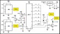
Decoder Encoder With 4017 Circuit Without Microcontroller.
- Thread starter KRAB
- Start date


| Thread starter | Similar threads | Forum | Replies | Date |
|---|---|---|---|---|
| K | Decoder encoder using 4017 with IR LED For transmitter | General Electronics Chat | 14 | |
| D | HOLTEK encoder and decoder | Wireless & RF Design | 9 | |
|
|
Encoder and decoder for remote control (RC car) | Digital Design | 17 | |
| I | Encoder/Decoder (Logisim) | Homework Help | 1 | |
| A | encoder/decoder Ir/Rf remote control | General Electronics Chat | 1 |


