Facebook
 Google
 GitHub
 Linkedin
Hello,
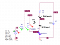
I do a simulation on the attached schematic. The input is 12-0V square wave with 50% duty cycle at f=8kHz. I want to know the Q1's collector current waveform, so I connect R3 = 1 ohm, and measure the voltage across it. As you can see, when the input is 12V, V+ - V- = 450mV. This means there is a current from the left pin of R3 to the right pin.
My question:
When Vin =12V, does this mean the current of Q1 flow from emitter to collector? If so, why does the NPN transistor carry such a current?
Thank You
BlackMelon
Attachments
-
 368 KB Views: 29