D Flip-Flop Frequency Divider

Thread Starter

genehorr

Joined Feb 28, 2019
8
I am trying to configure a D-type Flip Flop (TI CD4013BEE4) as a frequency divider off the output of a 555-style timer. The last time I worked with these types of circuits was during the 1st Reagan administration and have slept a few times since then. Ultimate goal is a square wave 50% duty cycle +/- 1% signal at .05 Hz (20 seconds per cycle). I tried doing this with just the timer but was never able to get the duty cycle accurate enough.

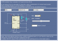
I am testing with a .5 Hz input signal at 5V. Power supplied to the chip is 5V. Searching with Google I find a plethora of block diagrams but very few actual schematics. The ones I found all contradict each other and/or contradict the datasheets for the chip. I am using the basic design for a 1/2 frequency divider: Output from the 555 into the clock line, D line tied to Q-Bar, Q as output, +5V to Set and Reset. 1KOhm resisters are on all input signal lines per the datasheet to limit current below 10mA. (Resisters on Clk line, on line between D and Q-Bar, and on S & R lines). This results in the output going high and never changing.

Some discrepancies from my searches:

1) S & R have +5V on some designs, some have them connected to ground.
2) Resister use and location are all over the place. Some have them, some don't.

This is a project that I am doing for free for a friend and so was trying to just use parts I had handy and only purchase a 555 and a 4013. Ultimate output is controlling a relay for a DC motor controller. Limit switches were not appropriate for this particular project and so I decided to just use a timer to control the back and forth motion of the motor.

Could someone please either give me a link to an appropriate schematic or tell me what I am doing wrong?
 

dl324

Joined Mar 30, 2015
18,260
Welcome to AAC!
1) S & R have +5V on some designs, some have them connected to ground.
Set and reset are HIGH active on CD4013.
2) Resister use and location are all over the place. Some have them, some don't.
Post a schematic so we know what you're referring to.
EDIT: corrected quoting problem.

If you don't intend to use set or reset, you can tie them to the appropriate supply without a resistor. Adding a pull-down resistor gives you the option of using them later. Hardwiring to a supply would preclude that...

To get divide by two, just connect the Q# output to D and tie (or pull down) set and reset to ground.

Ultimate output is controlling a relay for a DC motor controller.
CD4013 outputs can't drive mechanical relays directly.
 
Last edited:

Thread Starter

genehorr

Joined Feb 28, 2019
8
Thanks everyone for the tips and the link to the schematic. Also good idea on warning me about the output not driving a relay. I already had a power transistor in-between. I had omitted it from the description. Kind of a long story but the motor controller theoretically could accept TTL level switching but the power transistors I had on hand would only go down to about 30 Ohms and wouldn't work and so as a kludge just had one control a 12V relay which did work. The whole system is being run from a 12V battery with a 12V->5V power supply for the timing circuitry. It looks like I could run everything but the final power transistor at 12V but wanted to get everything working at a "safe" 5V before trying variants.

Regarding the 50% duty cycle on the 555 I will play around with that further. I was able to get 50% with a non-TI 555 timer but knocked the breadboard off the table and shorted something out <g>. It would not work with the TI though. I read something about people having problems with very low frequency circuits and so just gave up and used a 4013 as it should work without any fiddling. I'll post the final results here in case anyone else is researching the same problem/making the same mistakes
 

Thread Starter

genehorr

Joined Feb 28, 2019
8
The resistors and the reset and set lines were the causes of the problem. Once I changed those everything worked as it should.

Without wandering too much off topic the prior timer I used was a Maxim ICM7555. In the datasheet <https://www.mouser.com/datasheet/2/256/ICM7555-ICM7556-1292428.pdf> on page 6, figure 1(a) has a design for a single transistor 50% duty cycle circuit that is simpler to use with the lower power CMOS timers. Until I ruined that chip I can confirm that the design did work.

Will this design also work with the TI CMOS timer TLC555CP?

Again, I do appreciate the help. I do realize that these are issues that anyone who passed a high school (or maybe even junior high) course should know. Unfortunately Google searches return hundreds (thousands) of sites discussing theory and the few actual application sites are either misleading or apparently outright wrong.
 

dl324

Joined Mar 30, 2015
18,260
Glad the circuit is working. If you have the space for the flip flop, I'd always opt for using a toggle flip flop to get a 50% duty cycle. That will always work without tweaking.
Unfortunately Google searches return hundreds (thousands) of sites discussing theory and the few actual application sites are either misleading or apparently outright wrong.
Welcome to reality. Contrary to what too many gullible people think, just because it's on the Internet doesn't mean it's true.
 
Last edited:

crutschow

Joined Mar 14, 2008
38,391

Thread Starter

genehorr

Joined Feb 28, 2019
8
It should.
But it may not be as close to 50% as the flip-flop will give.
Thanks. I was trying to think of ways to simply things. I will just keep the flip-flop. On the subject of simplification - I am trying to think of a way to eliminate the 12V -> 5V power board. From what I've read the 555 and the 4013 will run off of 12V.

1) What would need to change on the IC sections? In particular I am thinking of the 555 output -> 4013 clock line. Does that become 12V now and is that voltage OK for the 4013?

2) Does the Q output of the 4013 now become 12V? If so I will need to drop that to 5V for the power transistor. I was assuming two resistors in series and tie across one of the resistors to lower the voltage as the easiest method if that is required.
 

crutschow

Joined Mar 14, 2008
38,391
1) What would need to change on the IC sections? In particular I am thinking of the 555 output -> 4013 clock line. Does that become 12V now and is that voltage OK for the 4013?
Yes, CD4000 series logic can operate from a 3V to 18V supply.
2) Does the Q output of the 4013 now become 12V? If so I will need to drop that to 5V for the power transistor. I was assuming two resistors in series and tie across one of the resistors to lower the voltage as the easiest method if that is required.
The 4013 output will be equal to the supply voltage.

What power transistor?
You wouldn't have to reduce the voltage for a MOSFET, but perhaps only adjust the base resistor if it's a BJT.
 

Thread Starter

genehorr

Joined Feb 28, 2019
8
What power transistor?
You wouldn't have to reduce the voltage for a MOSFET, but perhaps only adjust the base resistor if it's a BJT.
2N6292. From the datasheet max to the base is 5.0V. Max to the Collector is 70V which isn't a problem. Or am I misreading it?
Mod: Added the d/s.E
 

Attachments

Last edited by a moderator:

bertus

Joined Apr 5, 2008
22,906
Hello,

The mentioned 5 Volts in the datasheet is the reverse voltage on the base.
A BJT will always need a resistor in the base to limit the current.
The BE voltage will usualy be in the range of 0.6 to 0.7 Volts.

Bertus
 

Thread Starter

genehorr

Joined Feb 28, 2019
8
Hmm. More to study/learn. I had 5V to the base (with a 300 Ohm resistor) from the 4013, +12V to the relay (160 Ohms) then to the collector, and emitter to ground after misreading the datasheet. Everything worked and so I assumed I had it correct.

When I first was testing the transistor to see whether it would work I attached an ohmmeter across the collector and emitter and applied voltage to the base. I don't remember whether I had the emitter grounded to the power supply. The resistance measured in the megaohm range with no voltage and decreased to a few ohms at 5V. This also led me to assume I was doing it correctly.

I should know by now to be careful of those assumptions. They can bite you in the rear.
 

bertus

Joined Apr 5, 2008
22,906
Hello,

The sinking current of the cmos chip 4013 is very limited.

4013_sinking current.png
The 4013 can bearely supply 2 mA at the 5 Volts power supply.
Using a 330 Ohms resistor in the base of the transistor, you would draw 13 mA.
The output voltage will drop very low in this condition.

Bertus
 

Attachments

Thread Starter

genehorr

Joined Feb 28, 2019
8
I've got the ICs working at 12VDC. I am having trouble getting the transistor to work. All it is allowing through is a few mA. What is the easiest interface between the ~11.9V Q output of the 4013 and the base of the 2N6292? Load on the collector is 160 Ohms @ ~12.3V.

Edit: PS - I suspect the problem is that I went too far in trying to limit the current out of the 4013 and so there is now not enough current to the base of the transistor. Is my WAG in the ballpark or is it a case of "Er, transistors don't really work that way."?
 
Last edited:

dl324

Joined Mar 30, 2015
18,260
PS - I suspect the problem is that I went too far in trying to limit the current out of the 4013 and so there is now not enough current to the base of the transistor. Is my WAG in the ballpark or is it a case of "Er, transistors don't really work that way."?
You need about 7.5mA of base current; which is about twice what the device can source.

For a single transistor, we assume beta for saturation mode operation to be 10 (or 20 for high beta transistors like BC547).

You can use a darlington configuration to increase current gain. Or use an N channel MOSFET.

EDIT: Stated betas are for general purpose transistors. It will be lower for power transistors. The datasheet should give the appropriate beta for saturation mode operation.
 
Top