Current Analysis for Switched Supply - Please check

Thread Starter

Electronic_Maniac

Joined Oct 26, 2017
253
Hi All,

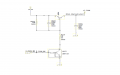
Please consider my circuit and check whether I have calculated my current correctly.
Please check the order of my steps and approach is correct. I am trying to do it accurately.

Part Number of Q114 - https://www.onsemi.com/pub/Collateral/MMBTA55LT1-D.PDF
Part Number of Q103 - https://assets.nexperia.com/documents/data-sheet/PDTC123J_SER.pdf

The load current of the circuit .i.e. Collector current of Q114 is 30mA (which I have calculated previously)
Apart from this load current of 30mA, I need to calculated the current in this 3.3V Rail for which I have calculated below.

1. Minimum Resistance of R139 = 950Ohms
2. Maximum Resistance of R139 = 1050Ohms
3. Maximum Input Voltage = 3.3 * 1.02 = 3.366V (Considering 2% tolerance)
4. Minimum Input Voltage = 3.3 * 0.98 = 3.234V (Considering 2% tolerance)
5. Maximum Load current through the collector Q114 Ic = 30mA
6. Maximum Collector Emitter Voltage Q114 Vce(sat) = 0.05V (Taken from Fig.6 graph in the datasheet for 150degC)
7. Minimum Base current Q114 Ib = Min Input Voltage/Max Resistance = 3.234/1050 = 3.08mA
8. Base Emitter Voltage of Q114 Vbe = 0.88V (Taken from Fig.7 graph in the datasheet for -55degC)

9. Collector Emitter Voltage of Q103 Vce = 0.045 (Taken from Fig.7 graph in the datasheet for +100degC) (Since the collector current of Q103 is the base current of Q114 = 3.08mA)

10. Maximum Current = (Max Input Voltage - Vbe of Q114 - Vce of Q103)/Min Resistance of R139 = (3.366-0.88-0.045)/950 = 0.002569474 ~= 2.5mA.

Please check my work. I have attached my circuit. Your feedback will be really helpful to me.

Thanks.
 

Attachments

wayneh

Joined Sep 9, 2010
17,496
You might consider simulating the circuit, for instance in LTspice. If you've never used it, there is a learning curve that's annoying but that time investment pays off quickly.
 

ebp

Joined Feb 8, 2018
2,332
It all looks correct. As for approach, I would do it almost in reverse order - start with the required output collector current for Q114 and work my way back to the value base resistor. It sort of looks like you have already done that and are going through the steps to confirm you choice is reasonable.

My only caution is with regard to temperature. Study the graphs of gain for Q114, and note that the DC gain is considerably higher at high temperature. The base-emitter voltage is also varies by around -2 mV/°C. These can be important considerations in selecting the base resistor if you need to operate over a wide temperature range. To be sure of adequate base drive at lower temperature, you may need to at least double the current you would use at high temperature. Many people use a rule of thumb of base current equal to 1/10 of collector current when using a transistor as a switch. This "rule" has come about because the saturation voltage at 25 °C is specified using that ratio. I don't like the rule - often you needlessly use higher base drive than necessary but sometimes you need even more base current. It is important to realize that the graphs are "typical" performance and you often need to design for "worst case" which means comparing the minimum, typical and maximum (not always spec'd) gain figures from the tables of data and what appears on the graphs. That may well lead you to conclude that the lowest gain at the lowest temperature you need to work at will be half or less of what the typical curves show for that temperature. It's a bit tedious.

Often you can ignore the tolerance of resistors in this type of circuit, but it is very good that you are aware of tolerances and know how to do the calculations. In other types of circuits, considering resistor tolerance is very important.The temperature coefficient of resistance can be a big issue, too (something that can mean you need to pay 10 or 20 times as much for a resistor to get the required characteristics), but not for this sort of circuit.

The same cautions about typical versus limit values apply when using simulation unless the models for the parts contain sufficient information and you know how to tell the simulator to do the required things. I don't use LTspice, so I don't know how complete the models are. Simulation is a great tool, but you must learn about its limitations and keep them in mind to be sure you don't draw inaccurate conclusions. There are several people at AAC who are very knowledgeable about LTspice.
 

Bordodynov

Joined May 20, 2015
3,177
Minimum Base current Q114 Ib = Min Input Voltage/Max Resistance = 3.234/1050 = 3.08mA is Bad!
Ib_min (Input Voltage-Vbe-Vsat_npn)/Max Resistance-Vbe/10kOhm = (3.234-0.88-0.1)/1050-0.88/10kOhm=2.06mA
 
Last edited:

Thread Starter

Electronic_Maniac

Joined Oct 26, 2017
253
It all looks correct. As for approach, I would do it almost in reverse order - start with the required output collector current for Q114 and work my way back to the value base resistor. It sort of looks like you have already done that and are going through the steps to confirm you choice is reasonable.

My only caution is with regard to temperature. Study the graphs of gain for Q114, and note that the DC gain is considerably higher at high temperature. The base-emitter voltage is also varies by around -2 mV/°C. These can be important considerations in selecting the base resistor if you need to operate over a wide temperature range. To be sure of adequate base drive at lower temperature, you may need to at least double the current you would use at high temperature. Many people use a rule of thumb of base current equal to 1/10 of collector current when using a transistor as a switch. This "rule" has come about because the saturation voltage at 25 °C is specified using that ratio. I don't like the rule - often you needlessly use higher base drive than necessary but sometimes you need even more base current. It is important to realize that the graphs are "typical" performance and you often need to design for "worst case" which means comparing the minimum, typical and maximum (not always spec'd) gain figures from the tables of data and what appears on the graphs. That may well lead you to conclude that the lowest gain at the lowest temperature you need to work at will be half or less of what the typical curves show for that temperature. It's a bit tedious.

Often you can ignore the tolerance of resistors in this type of circuit, but it is very good that you are aware of tolerances and know how to do the calculations. In other types of circuits, considering resistor tolerance is very important.The temperature coefficient of resistance can be a big issue, too (something that can mean you need to pay 10 or 20 times as much for a resistor to get the required characteristics), but not for this sort of circuit.

The same cautions about typical versus limit values apply when using simulation unless the models for the parts contain sufficient information and you know how to tell the simulator to do the required things. I don't use LTspice, so I don't know how complete the models are. Simulation is a great tool, but you must learn about its limitations and keep them in mind to be sure you don't draw inaccurate conclusions. There are several people at AAC who are very knowledgeable about LTspice.
Thanks ebp. Yeah. It is a design that has been made already and I am just performing some worst case calculations. Can you please explain me, what are the considerations that I have to take, if suppose I perform this design from from the beginning.

For example.. If the load current is the same 30mA, On what factors should I check while choosing a transistor and how should I choose the base resistor?
Can you please explain in simple terms? How to choose the components and values. I dont know on what basis the value of the resistor is chosen and why that transistor is chosen. Please explain.
Thanks
 

Thread Starter

Electronic_Maniac

Joined Oct 26, 2017
253
Minimum Base current Q114 Ib = Min Input Voltage/Max Resistance = 3.234/1050 = 3.08mA is Bad!
Ib_min (Input Voltage-Vbe-Vsat_npn)/Max Resistance-Vbe/10kOhm = (3.234-0.88-0.1)/1050-0.88/10kOhm=2.06mA
One small doubt.. But only the current that flows through the base of the transistor is called base current right?
Why are you considering the current through the 10K Resistor branch? That doesnt form a part of base current as it does not flow through the base right?
 
Top