Common Emitter Amplifier

Thread Starter

345wspo

Joined Jul 10, 2020
15
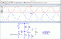
I found this ce amplifier in a textbook. If I simulate the circuit I get an o/p of 210 mV with a 1 mV sine input.
If I input a 10mV sine then the o/p is all distorted. The input rides on a base voltage of 2.0 and the output
rides on a dc level of 13.3 v. Why is it distorted?

1598879497435.png
 

ericgibbs

Joined Jan 29, 2010
18,734
hi 345,
This what I see on Vin and Vout for a 10mV sine input,
If you measure at the Base and Collector of the transistor, you will measure the values you quote.

E
 

Attachments

LvW

Joined Jun 13, 2013
1,749
When the DC level at the base is 2 Volts, the emitter node has a voltage of app. 1.3V across 1.5 kOhms. Hence we have an emitter current of 1.3/1.5k=0.87 mA. The DC voltage at the collector schould be app. Vc=22-0.87*10=13.3 V.
So - everything looks good. The gain should be app G=-gm*(10k||22k) with gm=0.87mA/26mV.
 

Jony130

Joined Feb 17, 2009
5,487
Why is it distorted?
Why? In short, you see a "distortion" because the BJT's is a nonlinear device and the voltage gain is not constant but it changes together with the Ic current exponentially.

Av = Vout/Vin = -Rc*Ic/Vt (with CE capacitor across RE ressitor)

Where Vt = 26mV is a Thermal Voltage

In your case, the midpoint gain is Av ≈ 38*Icq*(Rc||RL) = 38*0.87mA*(10kΩ||22kΩ) = 38*0.87mA*6.8kΩ = 224 V/V

Buy at the positive peak when Ic ≈ 0.87mA -10mV* (0.87mA/26mV) ≈ 0.535mA the gain is 6.8kΩ*0.535mA*38 = 138 V/V

And the voltage gain at the negative peak is Ic = Icq+10mV* (0.87mA/26mV) = 1.2mA --->Av = 38*1.2mA*6.8kΩ = 310 V/V

As you can see you amplifiers voltage gain changes together with the input signal by 38% so we can expect the THD te to be around 38/3 = 12%

You can improve the distortion by adding an external emitter degeneration resistor (without CE capacitor).
But to get "low THD" you need to pick RE >> re thus it is impossible to get high voltage gain and low THD in such a simple circuit.
 
Last edited:

crutschow

Joined Mar 14, 2008
34,201
there is thd of 8.3%
The distortion is due to the non-linear relation between the base current vs. the base-emitter voltage.
If you add some negative feedback (at the cost of a loss in gain), then the distortion will be smaller.


For example, adding an unbypassed emitter resistor of 100 ohms reduces the THD to <0.5% (below).
It also reduces the gain to about 50.

1598884415723.png
 

Thread Starter

345wspo

Joined Jul 10, 2020
15
The distortion is due to the non-linear relation between the base current vs. the base-emitter voltage.
If you add some negative feedback (at the cost of a loss in gain), then the distortion will be smaller.


For example, adding an unbypassed emitter resistor of 100 ohms reduces the THD to <0.5% (below).
It also reduces the gain to about 50.

View attachment 216054
 
Last edited:

Papabravo

Joined Feb 24, 2006
21,094
The selection of the bias point seems to be contributing to the distortion. Wouldn't a better bias point be located near Vcc/2?
 

LvW

Joined Jun 13, 2013
1,749
Why? In short, you see a "distortion" because the BJT's is a nonlinear device and the voltage gain is not constant but it changes together with the Ic current exponentially.

Av = Vout/Vin = - (Rc * Is)/Vt * exp^(Vin/Vt) (with CE capacitor across RE ressitor)

Where Vt = 26mV is a Thermal Voltage
Hi Jony130 - I am afraid that you have mixed Vin with the DC value Vbe.
The given formula cannot be correct.
I am sure you agree that the gain formula for very small input signals Vin is Av=-Rc*Ic/Vt.
When I insert very small values for Vin (app. Vin=0) in your formula we get Av=-Rc*Is/Vt. This result is obviously wrong.
 

yevgeny

Joined May 20, 2017
15
Crutschow is right. Problem is C3. That capacitor has it reactance impedance is paralleled RE, dramatically increase AC gain and reduce negative feedback which related directly to distortion (actually it is more complicated).

Yevgeny
 

LvW

Joined Jun 13, 2013
1,749
Crutschow is right. Problem is C3. That capacitor has it reactance impedance is paralleled RE, dramatically increase AC gain and reduce negative feedback which related directly to distortion (actually it is more complicated).
Yevgeny
But it is the task of C3 to increase the gain......that is its only purpose. If the distortion is to large, the classical method is to shunt only a part of the emitter resistor with a capacitor (the resistor must be split up in two resistors).
 

LvW

Joined Jun 13, 2013
1,749
When you split resistor, you increase total impedance (AC gain reduced).
Yevgeny.
Yes - thats what happens very often in electronics: We have to find a trade-of between two (or more) conflicting requirements.
In this case: Stability of the amplification factor and THD vs. gain.
 

Thread Starter

345wspo

Joined Jul 10, 2020
15
Yes - thats what happens very often in electronics: We have to find a trade-of between two (or more) conflicting requirements.
In this case: Stability of the amplification factor and THD vs. gain.
how did the designer compute the three capacitor values?
 

Audioguru again

Joined Oct 21, 2019
6,647
A transistor is very non-linear as it approaches cutoff. The gain is reduced so much that it squashes the top of the waveform even when it is far from clipping. I show the circuit without C3 so that there is plenty of negative feedback to reduce the gain and distortion, then I show it with C3 with high gain and high distortion.
 

Attachments

LvW

Joined Jun 13, 2013
1,749
how did the designer compute the three capacitor values?
It depends, of course, on the lowest frequency to be amplified. All three capacitors cause a high-pass behaviour.
The cut-off frequency for each R-C combination can be calculated - however, an experienced designer has a feeling for suitable values which are "on the safe side".
 

crutschow

Joined Mar 14, 2008
34,201
how did the designer compute the three capacitor values?
They are determined by the desired low-frequency rolloff.

The value of C2 is determined by that frequency and the parallel value of Rb1, RB2, and the transistor base input impedance rb.

The value of C1 is determine by that frequency and the parallel value of Rc and RL

The value of C3 would seem to be determined mainly by the value of RE and the frequency, but you must also include the value of the emitter output impedance, which is very low (≈ Ie/25mV @ room temperature).
Thus for the 50μF shown for the emitter bypass, the -3dB low-frequency point is about 100Hz.

So another reason to split the emitter resistor, to both reduce distortion and stabilize gain, is that you can use a smaller capacitor for a given low-frequency rolloff.
For example the 100Ω I used in my simulation reduced the LF rolloff to about 28Hz with a 50μF cap.

Note that the rolloff of the above three capacitors add together so you need to account for that to get the desired overall amplifier rolloff.
 

crutschow

Joined Mar 14, 2008
34,201
For those interested, here's the simulation showing the source of the distortion for the circuit with no emitter feedback.

As you can see, the transistor base-current (yellow trace) is quite non-linear versus input voltage (red trace), which thus causes the non-linear current (and output collector voltage) of the transistor (blue trace).
The transistor current-gain is essentially constant at this point, so is not a significant factor in the distortion.

1599013072782.png
 
Top