
Hi,
I have a problem on my 11 channel MOSFET based coil driver board. I have it programmed at the moment to cycle the output around the 11 channels then back to the start, with 3 channels active (50% duty) at any one time.
It works fine when I just have the LEDS switching on and off (no coil attached), but as soon as I connect a coil to one of the channels all other channels become partially active whenever that coil is powered. See Photo1 (normal behavior) and Photo2 (partially energised all channels)
I have my PWMs set to limit the current through the MOSFETs to about 2A. The PSU is set to 12V and has a current limiting function but I have it set unlimited for this test.
I don't have a scope, but I can see using my meter that on the channels that are partially high the gates of the MOSFETS are NOT being accidentally set high.
Voltage at the driven outputs are 12V as expected, and on the outputs that are unintentionally driven the voltage is 1.7V.
Any ideas please let me know.
OK behavior:

Bad Behavior:

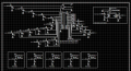
Schematic:

Close up on Channel layout:

Top Layer

Bottom Layer:

I have a problem on my 11 channel MOSFET based coil driver board. I have it programmed at the moment to cycle the output around the 11 channels then back to the start, with 3 channels active (50% duty) at any one time.
It works fine when I just have the LEDS switching on and off (no coil attached), but as soon as I connect a coil to one of the channels all other channels become partially active whenever that coil is powered. See Photo1 (normal behavior) and Photo2 (partially energised all channels)
I have my PWMs set to limit the current through the MOSFETs to about 2A. The PSU is set to 12V and has a current limiting function but I have it set unlimited for this test.
I don't have a scope, but I can see using my meter that on the channels that are partially high the gates of the MOSFETS are NOT being accidentally set high.
Voltage at the driven outputs are 12V as expected, and on the outputs that are unintentionally driven the voltage is 1.7V.
Any ideas please let me know.
OK behavior:
Bad Behavior:
Schematic:
Close up on Channel layout:
Top Layer
Bottom Layer:
Attachments
-
 101.2 KB Views: 15


