Circuit help

Thread Starter

Engineer_tech

Joined Sep 19, 2014
31
Hello to all
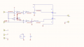
i am working on a driving circuit posted in the picture attached with this topic.
right now i wired up the circuit on board and tried to scope it i just need some help in understanding the flow of the circuit and if the output i am expecting is right or not.
so here is what i did please comment and correct me i applied a square pulse at the IN pin and just and enable switch at the EN pin.
when i scope the pin number 6 and pin number 4( of inverter) i am getting 5v pulse inverted to the pin number 6 pulse
what could be the expected output of this circuit.?
 

Attachments

MrCarlos

Joined Jan 2, 2010
400
Hello Engineer_tech

It is very easy to understand that circuit, or others, if you keep in mind the statement of the NAND gate:
Speaking of 1’s and 0’s.
Until all its inputs are 1 the output will be 0.
So any 0 on any input the output will be 1.

See the attached image. note how they appear the ones and zeros.

If everything works as expected, at the named terminal: XTALOUT and GND will have a voltage level changes from 12 to 0.

Probably required some resistors between the MOS-FET Transistors gates and their associated devices.
Also a resistor between the base of 2N2222 and associated AND gate is required.
 

Attachments

Thread Starter

Engineer_tech

Joined Sep 19, 2014
31
Hello Engineer_tech

It is very easy to understand that circuit, or others, if you keep in mind the statement of the NAND gate:
Speaking of 1’s and 0’s.
Until all its inputs are 1 the output will be 0.
So any 0 on any input the output will be 1.

See the attached image. note how they appear the ones and zeros.

If everything works as expected, at the named terminal: XTALOUT and GND will have a voltage level changes from 12 to 0.

Probably required some resistors between the MOS-FET Transistors gates and their associated devices.
Also a resistor between the base of 2N2222 and associated AND gate is required.
thanks Carlos for your reply
i just have a lit bit of mis understanding.lets say when the transistor 2N2222 is in on state means there is 1 at its base. the output will be zero
but when the transistor is in OFF state the voltage at the gate of MOSFET would be 12V?isnot it?
when i scope the collector of the transistor 2N2222 i am getting a pulse with 0-5V.
am i missing something or there is something shorted in the circuit which make the output at collector pin 0-5V pulse?
 

MrCarlos

Joined Jan 2, 2010
400
Hello Engineer_tech

You're saying:
When the transistor 2N2222 is in on state means there is 1 at its base. the output will be zero.
Yes, of course.

You're asking:
But when the transistor is in OFF state the voltage at the gate of MOSFET would be 12V ? isnot it ?.
Yes, of course. upper MOSFET gate should be about 12 V.

You're Asking:
when I scope the collector of the transistor 2N2222 I am getting a pulse with 0-5V.
am I missing something or there is something shorted in the circuit which make the output at collector pin 0-5V pulse ?


Just a question for You:
You are simulating that circuit? . . What simulator is?. . .
If you're simulating, surely because is the answer of your simulator.
Take a look at the picture I attached.
The red line on the face of the scope is the signal at the collector of the 2N2222.
There are 12 volts on the signal peak.
Also notice the blue line. At this point you can never get more than about 0.7 volts because the base-emitter junction.

Probably in your simulator options you have programmed for the power supplies that only provide 5 Volts.
But it can also be a failure of your simulator.

I use Proteus ISIS.
What simulator you are using?.
So I think you're not missing anything.
 

Attachments

Thread Starter

Engineer_tech

Joined Sep 19, 2014
31
Hello Engineer_tech

You're saying:
When the transistor 2N2222 is in on state means there is 1 at its base. the output will be zero.
Yes, of course.

You're asking:
But when the transistor is in OFF state the voltage at the gate of MOSFET would be 12V ? isnot it ?.
Yes, of course. upper MOSFET gate should be about 12 V.

You're Asking:
when I scope the collector of the transistor 2N2222 I am getting a pulse with 0-5V.
am I missing something or there is something shorted in the circuit which make the output at collector pin 0-5V pulse ?


Just a question for You:
You are simulating that circuit? . . What simulator is?. . .
If you're simulating, surely because is the answer of your simulator.
Take a look at the picture I attached.
The red line on the face of the scope is the signal at the collector of the 2N2222.
There are 12 volts on the signal peak.
Also notice the blue line. At this point you can never get more than about 0.7 volts because the base-emitter junction.

Probably in your simulator options you have programmed for the power supplies that only provide 5 Volts.
But it can also be a failure of your simulator.

I use Proteus ISIS.
What simulator you are using?.
So I think you're not missing anything.
Thanks Mr.Carlos your detailed reply was very helpful i can now easily figure out my circuit and the behavior expected from all transistors and FETs
well i didn't use any simulator i just wired up the circuit on bread board and tried to scope it.i guess now i have to go through and rewire the circuit again because of transistor and fets heating up i think one of the device is not working anymore.
can you suggest me some modifications in the circuit coz the nand gate IC and Fets heat up alot in few second?
i believe you suggested me to have an base resistance at base of transistor what other modifications you think i should look for ?

thanks for taking time out and helping me out.
 

MrCarlos

Joined Jan 2, 2010
400
Hello Engineer_tech

Probably the transistor and IC are heated by excessive current flowing in the emitter-base junction of the transistor and the output of AND gate U1B in Your circuit.
At this point is where I recommended that you added a resistor, say 4.7K.

Currently I do not know what the value of Vcc. for the IC.
Assuming were 9V. So about 2mAmp. Is the current flowing through the base-emitter junction (IB).
(9/4700 = 2mAmp).

If the 2N2222 has a gain of 100 then the IC (collector current) would be 0.002 x 100 = 100mAmp.
But I do not know the electrical characteristics of the transistor.

I guess with a collector resistor of about 10K would be enough to bias the MOSFET you look at the top of your design.

And this is only for the bipolar transistor 2N2222. Also missing check the electrical characteristics of MOSFET transistors.

However I think that with these changes, no longer will heat the devices in your design.
Any information on the electrical characteristics of the components that you use in your design you can find them at this link.
http://www.alldatasheet.com/
For example:
How much power can supply the NAND gates that you use.
The NOT gate that looks into your scheme, can handle directly the MOSFET ?
The MOSFET transistors, can handle what connect where they join ?
In general terms, it is necessary to know the electrical characteristics of each device to see if ‘one can handle the next’.
 
Top