And i didnt get it. People here are saying it causes hysteresis. You dont say that. Also resistor r5 can be removed and circuit still switch on and off. I still dont get it how is it switching faster. I wouldnt have reposted if i had understood it. Please help
For starters, if R5 is removed the LED will only gradually come ON as the V2 voltage starts to rise above 0.6 volts
R5 provides a path for positive voltage feedback to the base of Q2 to rapidly saturate the transistor ON so the LED appears to be fully lit immediately at the 0.6 volt threshold.
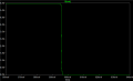
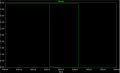
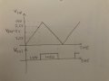
Top trace is input. (0.5V to 0.7V)
Middle trace is the output with no Schmitt trigger action. The red line is the on/off point.
The bottom trace is the output with Schmitt Trigger. On the way up the trip point is the top green line. On the way down the trip point is the bottom green line.
For starters, if R5 is removed the LED will only gradually come ON as the V2 voltage starts to rise above 0.6 volts
R5 provides a path for positive voltage feedback to the base of Q2 to rapidly saturate the transistor ON so the LED appears to be fully lit immediately at the 0.6 volt threshold.
Based on what? I'd really like to know -- I might learn something about some kind of LED light that's out there.
But, for now at least, I'll assume that it really does, somehow, through some magic, behaves like a 60 Ω resistor.
For the moment, let's ignore the effect R5, either by removing it or making it so large that it might as well be removed. Then let's look at how we expect the circuit to behave using a very simplified model of the transistors.
My transistor model is beta = 100, Vbe = 0.7 V, Vcesat = 0 V.
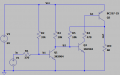
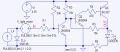
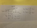
I redrew your schematic so that it makes more sense (at least to me):
Looking at the output stage (Q3 and LED), if Q3 is fully saturated, which we will assume let's it produce Vce = 0 V, then we will have 100 mA in the LED and a base current of 1 mA.
If Q2 is fully saturated, then the voltage across R4 is (6 V - 0.7 V) - (0 V) = 5.3 V, yielding a current of 11 mA, more than enough to saturate Q3, which will require a base current of ~100 µA in Q2.
To turn Q2 on, V(b2) has to be 0.7 V, which requires a current of 530 µA in R3, of which 100 µA will flow to Q2 and the rest, about 400 µA, will flow down through Q1, requiring a base current in Q1 of about 4 µA.
To turn on Q1, V(b1) has to be 0.7 V, which will require a current of 160 µA in R2. Compared to this, the 4 µA that goes to Q1 is pretty negligible, so we'll assume that it all flows through R1, which puts the voltage a V(in) needed to turn on Q1 at
V(in) = 0.7 V - (270 Ω)(160 µA) = 657 mV.
This represents the theoretical point between on and off. If we use different model parameters, say Vbe = 0.6 V and beta = 300, we will get a different value of V(in), but this is probably within, say, 50 mV.
What happens if Vin is above this threshold?
That will result in more base current in Q1, which will put it deeper into saturation. This will rob Q2's base of current, which will pull it out of saturation and thus reduce Q3's base current, which will reduce the LED current.
What happens if Vin is below this threshold?
This will result in less base current in Q2, which will reduce the collector current, which will increase the base current in Q2, driving it deeper into saturation, which will (try to) increase the LED current.
Now, what happens when R5 is put into the circuit?
Let's review how this thing turns on and turns off the LED.
To turn it on off, Q1 is turned off on, thereby stealing the base current of Q2. The base current that it has to steal is the 530 µA flowing in R3 so that all of that current is flowing through Q1 and none of it can flow into Q2's base.
But, with R5 in place, when the LED is fully on, there is another 10 Ω resistor that has 5.3 V across it, yielding another 530 µA of current available to Q2, so not Q1 has to steal twice the current in order to make this happen, which is going to require that V(in) be even higher to turn the LED off.
On the flip side, to turn the LED on, V(in) is reduced until Q1 starts coming out of saturation. This makes some of the current in R3 available to Q2's base. So let's assume that V(in) is carefully adjusted so that it is just resulting in enough current into Q2's base to just start turning on Q3. But now what happens? As Q3 starts turning on, some of the current coming out of it's collector goes through R5. Since Q1 is operating in a constant current mode, all of that current has to go into Q2's base, which means that it pulls down harder on Q3's base, resulting in even more collector current, which results in even more current in R5, which results in Q2 pulling down even harder. This is positive feedback. The result is that as soon as V(in) rises up just enough to get almost any current flowing through Q3, this positive feedback mechanism drives Q2 and Q3 rapidly into saturation.
But now what happens when we tray to turn the LED off again? We've carefully set V(in) to the voltage where, without R5, Q3 would be just on the verge of turning on, but there would only be a tiny bit of current available to it (not nearly enough to light it up). But with R5, the LED has lit up due to the positive feedback. However, raising V(in) just a little bit won't shut the LED back off, because it is just barely at the point to pull 530 µA from Q2's base. But now, thanks to R5, we have to raise it enough to pull over 1000 mA from it. This is the source of the hysteresis.
So how does this square up with the simulations of the circuit?
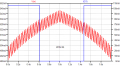
Let's first simulated it without R5 (or with R5 set to 10 MΩ instead of 10 kΩ)
We can see that the threshold is right around 596 mV, or about 40 mV higher than our super-simple model predicted. Not bad.
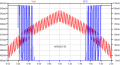
Now let's set R5 to the 10 kΩ in the schematic:
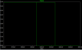
Here we see that the turn-on threshold has barely moved, to perhaps 594 mV, but the turn-off threshold has moved up to about 613 mV.
If we lower R5 further, this hysteresis would increase. Here's what it looks like with R5 set to 1 kΩ.
It was calculated by using a hfe or gain of appx 11 for Q2.
R3 and R5 are essentially in parallel with a total resistance of 5K providing bias for Q2 which is appx 11X the value of R4
R4 determines the bias for Q3.
Using a gain of 11 for Q2 which is well above the minimum spec required allows a bias current of appx 11X less then the bias current through R4.
Based on what? I'd really like to know -- I might learn something about some kind of LED light that's out there.
But, for now at least, I'll assume that it really does, somehow, through some magic, behaves like a 60 Ω resistor.
For the moment, let's ignore the effect R5, either by removing it or making it so large that it might as well be removed. Then let's look at how we expect the circuit to behave using a very simplified model of the transistors.
My transistor model is beta = 100, Vbe = 0.7 V, Vcesat = 0 V.
I redrew your schematic so that it makes more sense (at least to me):
Looking at the output stage (Q3 and LED), if Q3 is fully saturated, which we will assume let's it produce Vce = 0 V, then we will have 100 mA in the LED and a base current of 1 mA.
If Q2 is fully saturated, then the voltage across R4 is (6 V - 0.7 V) - (0 V) = 5.3 V, yielding a current of 11 mA, more than enough to saturate Q3, which will require a base current of ~100 µA in Q2.
To turn Q2 on, V(b2) has to be 0.7 V, which requires a current of 530 µA in R3, of which 100 µA will flow to Q2 and the rest, about 400 µA, will flow down through Q1, requiring a base current in Q1 of about 4 µA.
To turn on Q1, V(b1) has to be 0.7 V, which will require a current of 160 µA in R2. Compared to this, the 4 µA that goes to Q1 is pretty negligible, so we'll assume that it all flows through R1, which puts the voltage a V(in) needed to turn on Q1 at
V(in) = 0.7 V - (270 Ω)(160 µA) = 657 mV.
This represents the theoretical point between on and off. If we use different model parameters, say Vbe = 0.6 V and beta = 300, we will get a different value of V(in), but this is probably within, say, 50 mV.
What happens if Vin is above this threshold?
That will result in more base current in Q1, which will put it deeper into saturation. This will rob Q2's base of current, which will pull it out of saturation and thus reduce Q3's base current, which will reduce the LED current.
What happens if Vin is below this threshold?
This will result in less base current in Q2, which will reduce the collector current, which will increase the base current in Q2, driving it deeper into saturation, which will (try to) increase the LED current.
Now, what happens when R5 is put into the circuit?
Let's review how this thing turns on and turns off the LED.
To turn it on, Q1 is turned off, thereby stealing the base current of Q2. The base current that it has to steal is the 530 µA flowing in R3 so that all of that current is flowing through Q1 and none of it can flow into Q2's base.
But, with R5 in place, when the LED is fully on, there is another 10 Ω resistor that has 5.3 V across it, yielding another 530 µA of current available to Q2, so not Q1 has to steal twice the current in order to make this happen, which is going to require that V(in) be even higher to turn the LED off.
On the flip side, to turn the LED on, V(in) is reduced until Q1 starts coming out of saturation. This makes some of the current in R3 available to Q2's base. So let's assume that V(in) is carefully adjusted so that it is just resulting in enough current into Q2's base to just start turning on Q3. But now what happens? As Q3 starts turning on, some of the current coming out of it's collector goes through R5. Since Q1 is operating in a constant current mode, all of that current has to go into Q2's base, which means that it pulls down harder on Q3's base, resulting in even more collector current, which results in even more current in R5, which results in Q2 pulling down even harder. This is positive feedback. The result is that as soon as V(in) rises up just enough to get almost any current flowing through Q3, this positive feedback mechanism drives Q2 and Q3 rapidly into saturation.
But now what happens when we tray to turn the LED off again? We've carefully set V(in) to the voltage where, without R5, Q3 would be just on the verge of turning on, but there would only be a tiny bit of current available to it (not nearly enough to light it up). But with R5, the LED has lit up due to the positive feedback. However, raising V(in) just a little bit won't shut the LED back off, because it is just barely at the point to pull 530 µA from Q2's base. But now, thanks to R5, we have to raise it enough to pull over 1000 mA from it. This is the source of the hysteresis.
So how does this square up with the simulations of the circuit?
Let's first simulated it without R5 (or with R5 set to 10 MΩ instead of 10 kΩ)
Thanks. I am confused. When Q1 is off, how can there be no current through Q2 base? Why doesn't the current go-to Q2 base when Q1 is off? R3, R5, Q2 base, and Q1 collector are all at the same node so why wouldn't it? Also, if current doesn't go to Q2 base and Q1 is off, you said it goes through Q1, but Q1 is off. How can current go through Q1 at all? Where does the current go? I don't get that. Above are just a few questions as I began to read your input carefully. I have yet to read through all of it.
Thankyou Danko for going to the work to draw the schematic and show the results. That is work! You are better than I am.
I was going to do that but when hhstingis not going to spend 20 seconds to post the CAD file I am not going to spend 30 minutes to help.
Thankyou Danko for going to the work to draw the schematic and show the results. That is work! You are better than I am.
I was going to do that but when hhstingis not going to spend 20 seconds to post the CAD file I am not going to spend 30 minutes to help.
@hhsting
Nobody ask you about AutoCAD file.
CAD is Computer Aided Design.
Your LTspice is CAD program, because your
circuit designed with help of computer.
So, @ronsimpson asked you to send .asc file,
which contains information of your circuit.
Thanks. I am confused. When Q1 is off, how can there be no current through Q2 base? Why doesn't the current go-to Q2 base when Q1 is off? R3, R5, Q2 base, and Q1 collector are all at the same node so why wouldn't it? Also, if current doesn't go to Q2 base and Q1 is off, you said it goes through Q1, but Q1 is off. How can current go through Q1 at all? Where does the current go? I don't get that. Above are just a few questions as I began to read your input carefully. I have yet to read through all of it.
Thankyou Danko for going to the work to draw the schematic and show the results. That is work! You are better than I am.
I was going to do that but when hhstingis not going to spend 20 seconds to post the CAD file I am not going to spend 30 minutes to help.
What sort of "Electrical Engineer" is not able to understand the very detailed descriptions provided??? Hysteresis, and positive feedback??? What sort of educatio did not include that part of an EE education?????
What sort of "Electrical Engineer" is not able to understand the very detailed descriptions provided??? Hysteresis, and positive feedback??? What sort of educatio did not include that part of an EE education?????
I understand what hysteresis is ok from this forum. I just cant do calculations and equations to measure hysteresis and what voltage and currents go where due to complexity of the circuit itself.
Understand a transistor comparator is harder than a chip comparator. In transistor circuit you have to deal with currents “inside” the circuit and Vbe offsets, in chip all is already done and precise.
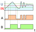
Try to look at schmitt trigger made from common comparator IC on picture below , in transistor comparator the basic is the same:
The corners of hysteresis VH and VL are set by R1 and R2 resistors ratio, (not the value of resistors), and the middle point is set with Vref. The 10V supply voltage is also important to obtain desired result:
So the comparator outputs High when Vin is >7.5V and flips to Low when Vin is <2.5V.
Btw, the feedback resistor R5 in your schematic is R2 in this schematic.
By feeding the Vin with 0-10V triangle the Vout output looks like this:

 Facebook
 Google
 GitHub
 Linkedin