 Facebook
 Google
 GitHub
 Linkedin
Hello, I don't know if this is the corret thread to publish this. If not, I apologize, but could you please tell me the right one? I'm new to this forum.
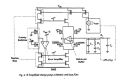
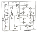
In my RF classes I was introduced the Charge pump and at some point we were given these two schematics I attached to this post.
Now, the first one is supposed to be the same as the second one, but on a higher-level system view.
SHORT QUESTION: I don't understand how this circuit works and how the first scheme translates into the second;
LONG QUESTION: this is what I understand of the circuit:
I don't understand how the circuit works. Let's take the second image. The sub-circuit to the far right is the charge pump. Now, let's call the On node "X".
As far as I understood, we use the feedback control and the replica bias in order to make sure that the "Vreplica" voltage in the "replica-bias" sub-circuit is identical to the voltage on X.
Now, why would I want that?
From what I understood, there seems to be a problem when Icp (the upper charge pump current) and Idown (the lower one) are different, so I thought "ok, maybe it works like this: if Vx rises, then the right transistor of the diff. couple in the feedback control drives more current. The couple's current is set at 2I by the multiple mirror (the couple's tail transistor is"2Wn" and there's a conversion ratio of 2, ideally). So this means that the left transistor of the couple shall drive less current.
Now, keep your eyes on the feedback control: if the right current of the couple rises, then the D-S voltage shall rise, too. This means that since the drain of the left transistor is linked to the gates of the upper transistors, the Drain voltage shall become the Gate voltage of all the P-MOSs in the upper frame of the picture.
Now: since gate voltage is increasing, the MOS which drives "Icp" (upper charge-pump current) should drive less current.
This also means, though, that on the far left (replica bias sub-circuit) the PMOS should drive less current.
This is what I do not understand: if the current decreases, the Vreplica voltage should decrease, right? Then what's the point of this thing? Shouldn't it be like to keep Vreplica= Vx?
And, btw, what happens when Vreplica=Vx? Why do we want this?
Furthermore, how do you get from the first scheme to the second one?
Thank you very much.
Attachments
-
 192 KB Views: 31
 -
 360.6 KB Views: 29


