Facebook
 Google
 GitHub
 Linkedin
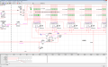
Shift register (S/R) CD74AC164 conditions:
Pin 1: +5V,
Pin 2: +5V until next 100 nsec CP - (sets Q0 (pin 3) high),
Pin 3: Stated above.
Pins 4 thru 6 and 10 thru 13: low,
Pin 7: Gnd,
Pin 8: 100 ns period CP, repetitive 72 ms,
Pin 9: Initially low, now high,
Pin 14: +5V
Initially, S/R was cleared (low), now high. Set the first bit (Q0) high, verified on scope. The CP that ended the Q0 bit did not transfer that bit to Q1. The period of the set bit is 72 ms.
My question: Why didn't Q0 (pin3) transfer to Q1 (pin 4)?
Thank you!!!
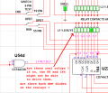