Can someone help with a pcb layout.

Thread Starter

martijndk1983

Joined Jul 26, 2015
21
Hello

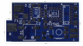
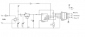
I have an circuit diagram and the original pcb board.
Now i want to let make some pcb boards but i need an pcb file and i really don't know how to make them, for me it is abracadabra.
So is there someone who can make an pcb file so i can send it to the manufacture and let make some prototypes.

This are the parts.
PIC 12F629-I/SN
µA 78L05 SMD
ULN 2003 AD SMD
1N 4148 SMD
HDBLS 103G
X7R-G1206 100N
X7R-G1206 1,0uf/50v
SMD 1/4W 22K
Zekering snel 2,0A(Geloof dat dit een 1808 is.)
button 9313

Thanks for youre time.
 

Attachments

jpanhalt

Joined Jan 18, 2008
11,087
Are you trying to reverse engineer that PCB so you can order duplicates? It looks like a single-sided board (no obvious vias). Can you confirm whether that is the case? If so, a brighter image probably can be photoshopped to a more readable example than that and be redrawn with any of the many programs available.
 

Thread Starter

martijndk1983

Joined Jul 26, 2015
21
Hello

It is an decoder for a model train.
It is from an guy that also has this hobby but I can't reach them.
No copyrighted or other licensed pcb's
 

jpanhalt

Joined Jan 18, 2008
11,087
First is little lesson in American law, as I understand it from years ago. Something that is copyrightable is copyrighted from the moment of creation regardless of whether a notice is given. That may not apply to where you are. My concern did not involve copyright per se.

My point was, if you do the Photoshop spade work, it will be much easier for someone to convert that image to a build-able PCB (i.e., Gerber files) for you. Speaking only for myself, I will not mess with something that is black and a very dark navy blue.

EDIT: I hope you realize those are all surface mount devices (SMD). For me, that is the preferred package, down to 805 size. For you, that may not be the case. Are you conformable with 805 or 1206-sized SMD's? ( I haven't checked which size is used.)
 
Last edited:

Thread Starter

martijndk1983

Joined Jul 26, 2015
21
Ahh oke,,

The size is 1206 except the fuse that is 1808, that is a nice size to soldering it.
What should i do in Photoshop, color the lines of connections and highlight what component is in witch place?
The input from the track is 16v till 18v.
 
Last edited:

Mark Hughes

Joined Jun 14, 2016
409
Hey @martijndk1983 -- I was just at DesignCon where a new website was launched: PCBLayout.com
I don't know too much about it yet -- but apparently if you send them the schematic, they create the PCB layout -- and then they can make the board for you, or you can have it made (by OshPark or similar).

@jpanhalt, I think that schematic has some German writing on it -- you don't happen to know the EU copyright laws do you? I've never investigated the issue myself.
 

jpanhalt

Joined Jan 18, 2008
11,087
@Mark Hughes,
German law appears to follow EU (https://iclg.com/practice-areas/copyright-laws-and-regulations/germany ) . There is no "fair use" provision per se. Thanks for pointing that out.

@martijndk1983
What I meant about Photoshopping was something with more color contrast that could be printed on a B&W laser printer. What is posted has traces and pads in dark blue and black with a background of very dark blue. For example, if the traces were red, it would be easier to copy. It looks like a fairly simple design with mostly large rectilinear signal pads rather than narrow signal paths.

I simply lightened and did some simple adjustments to get this:
upload_2019-2-3_7-41-49.png

Now, the copper stands out a bit better.

Mark's point about copyright is well taken. The schematic is not terribly unique, but the board arrangement might be considered that way. The bridge rectifier is in the Eagle CAD library as are the passive parts and voltage regulator. The other two IC's have a standard package . One would only need to create a symbol (very easy to do) to create those devices.

1) Unless there is a disclaimer, what you have is copyrighted by its original author. That copyright may have been transferred to something like a creative commons copyright. If so, that should be stated explicitly. For example, on the Adafruit and Sparkfun sites, you will notice a lot of products that those companies have put effectively into the public domain. Do you have evidence the original maker of this device has done the same?

2) My Eagle license is for educational and non-commercial use only. You mention making several. Is that for resale?

SUGGESTIONS:

1) Contact the manufacturer to determine copyright status.
2) Get a free CAD program. Kcad and Eagle would be my top two choices.
3) Create a usable schematic based on what you have and any changes you may want. I have a sense that schematics are hard to protect copyright on or not worth the effort for non-unique designs. If you check Adafruit and Sparkfun, you find many are "almost" identical to other works on the Internet, yet no one seems to mind.
4) Create your own board or use what you have based on what you find out on the copyright.

Regards, John
 

Thread Starter

martijndk1983

Joined Jul 26, 2015
21
There is no copyright or other protection on this board.
This board is just from a smart guy, no big company or something like that.

What should I do next?
Yesterday evening I spend several hours in drawing programs but I think I gone download eagle eye and try if I can draw it. But I have never done that.

Edit: i installed eagle but for me it is abracadabra.
Is there no program that can convert the scan to a print.
 
Last edited:

edwardholmes91

Joined Feb 25, 2013
210
Is there no program that can convert the scan to a print.
I'm not aware of any I'm afraid. Unfortunately, it really depends on what layers you want. There is usually a copper layer, solder mask and silkscreen for each side of the board.

I think you're probably best getting to grips with a schematic capture and PCB package first, then once you're happy with the process and how your chosen software works, you can input the design you want to duplicate.

I found a book called Build Your Own Printed Circuit Board - Al Williams quite useful, but a search on Amazon for 'How to make a PCB' reveals many similar books on the topic. I've never read them but the first 2 that came up in the search results: Jumpstarting Your Own PCB: Learn How to Design and Make Customized Circuit Boards - Shawn Wallace and also Make Your Own PCBs with EAGLE: From Schematic Designs to Finished Boards - Simon Monk & Duncan Amos look quite promising too.
 

Thread Starter

martijndk1983

Joined Jul 26, 2015
21
Hello

Thanks for thinking with me but this is for me once in my life that i need a design for a pcb,
i have now everything on place and want to draw the lines and pads. but it is me a pain in the ass.
upload photo.png

Edit: now i am drawing the lines but is this the right way to do the right layer etc, and is it not smarter to make them a other layer and place them later in the good one so that the color is other.
And on the original are whole copper fields, do they have a function transfer heat or something?
It is going to be a mess this way i think but i don't know if that is normal:D
Naamloos2.png

I cant upload the .pcb file or is there a way.
Not all the parts are the right one but i do my best tomorrow to find the right parts and make clear labels, maybe would someone look at the pcb file and do some editing if necessary
 
Last edited:

dl324

Joined Mar 30, 2015
16,846
Regarding copyright laws. In the US, artwork is automatically protected whether it contains a copyright mark or not. Most countries will honor the copyright laws of another country; with China being a notable exception.

In fairness to artwork creators, it's common courtesy to give attribution. When I post portions of datasheets or other information, I try to remember to give credit where credit is due.

If you copy a design, you should give attribution on your work. Otherwise, you could find yourself being sued.
 

Thread Starter

martijndk1983

Joined Jul 26, 2015
21
America has a other law then in the netherlands, here you can only protect youre stuf when it is written.
And it is a hobby project so there cant be protection on.

Someone in the netherlands helped me with drawing and the result is nice.
 

Attachments

jpanhalt

Joined Jan 18, 2008
11,087
Edit: now i am drawing the lines but is this the right way to do the right layer etc, and is it not smarter to make them a other layer and place them later in the good one so that the color is other.
Parts placement is usually key to good routing. In my opinion it is more difficult, but following some simple rules helps.

And on the original are whole copper fields, do they have a function transfer heat or something?
It is going to be a mess this way i think but i don't know if that is normal:D
Yes, those large copper areas can be needed for heat and current carrying capacity.

The routing you show has some notable errors. For one thing, IC2 is not properly connected. It is providing a lot of current and the interconnection of the pins is important.

I am not familiar with Design Spark. In Eagle, those copper areas are laid out as "polygons" and given signal names. You do not use simple geometric squares, rectangles and circles to make them.

Edit: I see you have improved IC2/IC3. Do those large red areas have signal names and are they connect to the pins or just laying under them/overlap?
 

dl324

Joined Mar 30, 2015
16,846
America has a other law then in the netherlands, here you can only protect youre stuf when it is written.
And it is a hobby project so there cant be protection on.
It's still a common courtesy to give attribution for the work of others.

In general, I don't mind if someone uses my designs for their own personal use. If someone benefits financially from my work, that's a different matter.
 

Thread Starter

martijndk1983

Joined Jul 26, 2015
21
It's still a common courtesy to give attribution for the work of others.

In general, I don't mind if someone uses my designs for their own personal use. If someone benefits financially from my work, that's a different matter.
I know what you mean but the oter guy has online the user guide, csv file, bom file, the schematic.
So i dont think it is a problem.

Now i have to look to convert a pcb to gerber format.
automaticly because is dont have knowledge of all the options in the software.
It looks not so easy as doing an png to img haha
 
Last edited:

jpanhalt

Joined Jan 18, 2008
11,087
I know what you mean but the oter guy has online the user guide, csv file, bom file, the schematic.
So i dont think it is a problem.
Then why not give a link to the original so its author can bask in the glory?

BTW:
martijndk1983 said:
America has a other law then in the netherlands, here you can only protect youre stuf when it is written.
And it is a hobby project so there cant be protection on.
It's a rather small point all things considered, but I checked the current copyright law in the Netherlands: https://www.blenheim.nl/copyright-law.html

Your law is quite similar to American and German law.
 

dl324

Joined Mar 30, 2015
16,846
Now i have to look to convert a pcb to gerber format.
automaticly because is dont have knowledge of all the options in the software.
It looks not so easy as doing an png to img haha
There aren't many components. If it were me, I'd enter the schematic in your favorite schematic editor and do a board layout from that. You already have a placement example, so it won't take long. You may even find that you can improve placement. If you do, you can provide the info to the original author as a consideration for being able to his design.
 

Thread Starter

martijndk1983

Joined Jul 26, 2015
21
i have now already a board layout, now is the problem to convert it.
Because the manufacture needs a gerber file.
And i thought i put it in the converter and done but also that is a bit difficult if you have never use pcb design etc before.
upload photo.png
 
Top