Building a DIY Regulated Buck Converter using no ICs (2)

Thread Starter

Nay007

Joined Oct 17, 2026
4
You do know that op amps and 555s are ICs(?).

The feedback loop for your circuit needs compensation to be stable due to the phase-shift of the L1C2 output.
Here are some articles on that.

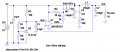
Below is the LTspice sim of a simple hysteretic type (bang-bang) buck-converter using a comparator, which does not require feedback compensation:
The output is shown for battery voltages of 16V, 20V, and 24V.
The output has ≤50mV of ripple at 0.5A load current:

View attachment 346208
Hello sir, I am brand new to circuits and decided to look at this circuit of yours to study over the past couple of days. I've learnt an incredible amount from this single schematic, but I can't for the life of me figure out how the upper and lower thresholds for hysteresis is formed? From my current understanding the output of the comparator will have an effect on its reference to create an upper and lower limit but I'm really not seeing it. Would you be able to explain this to me please?

Moderator edit: New thread created from this.
 

dl324

Joined Mar 30, 2015
18,490
Welcome to AAC!
From my current understanding the output of the comparator will have an effect on its reference to create an upper and lower limit but I'm really not seeing it. Would you be able to explain this to me please?
1792873187158.png
The comparator compares the output voltage with the reference voltage. When the output voltage is higher than the reference voltage, the comparator turns off the pass MOSFET. When the output voltage is lower than the reference voltage, the comparator turns it on.

The thread title is misleading because it would be a PITA to do this without using ICs.
 

crutschow

Joined Mar 14, 2008
38,909
how the upper and lower thresholds for hysteresis is formed?
It's basically determined by the values of L1, C2, and the load current.
There is otherwise no distinct/separate circuit to generate the hysteresis.
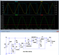
(LTspice sim below):
U1 turns off M1 (blue trace high) when the output (green trace) exceeds the Ref voltage (red trace), but the output voltage keeps rising due the the energy stored in L1 and its current (yellow trace) going into C2 (which is carried by D2 when M1 is off).

After the inductor current drops to zero and the load current causes the output voltage on C2 to drop below the Ref voltage, U1 turns M1 back on, starting an increase in the inductor current and repeating the cycle.

This causes an output ripple of about 30mVpp here with 5V nominal output for the shown values of L1, C2, and Rload.

Make sense?

1792875712950.png
 
Last edited:

Thread Starter

Nay007

Joined Oct 17, 2026
4
Welcome to AAC!

View attachment 372647
The comparator compares the output voltage with the reference voltage. When the output voltage is higher than the reference voltage, the comparator turns off the pass MOSFET. When the output voltage is lower than the reference voltage, the comparator turns it on.

The thread title is misleading because it would be a PITA to do this without using ICs.
Thanks, I've found AAC to be an actual goldmine. My question was specifically about how the upper and lower thresholds are established. Crutschow mentioned that this circuit uses hysteresis, giving a maximum and minimum voltage across the load before the PMOS switches state, preventing it from switching with a super high frequency. I'm confused with how those thresholds are set by the components in this circuit. Also, I appreciate you telling me that IC's make this much easier, because I've spent a crazy amount of time trying to understand this lol; It's very good for learning though, there was a lot to pick out.
 

Thread Starter

Nay007

Joined Oct 17, 2026
4
It's basically determined by the values of L1, C2, and the load current.
There is otherwise no distinct/separate circuit to generate the hysteresis.
(LTspice sim below):
U1 turns off M1 (blue trace high) when the output (green trace) exceeds the Ref voltage (red trace), but the output voltage keeps rising due the the energy stored in L1 and its current (yellow trace) going into C2 (which is carried by D2 when M1 is off).

After the inductor current drops to zero and the load current causes the output voltage on C2 to drop below the Ref voltage, U1 turns M1 back on, and the cycle repeats.

This causes an output ripple of about 30mVpp here with 5V nominal output for the shown values of L1, C2, and Rload.

Make sense?

View attachment 372651
This makes perfect sense, thank you so much! You used a filter which lets the voltage that the load experiences overshoot and undershoot. I'm unreasonably happy right now lol.
 
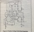
This type of regulator is called the hysteretic regulator. Although it is very straightforward and foolproof, it suffers from a couple of drawbacks:
-The output MUST HAVE RIPPLE for the regulator to operate.
-Its frequency is not fixed, it varies with load and line conditions.

There are improvements to be made to address these issues, Unitrode Corp published an app note U-68A in the mid 1980s, which describes in detail the operation, component selection, detailed design and performance characteristics.
It used a single uA723, which incorporates the reference, comparator, current limit and drive circuit in a single IC.

I actually designed a variant of figure 8, which was used commercially.
You can still see my pencil notes on the pages. IMG_2580.jpeg
 

Thread Starter

Nay007

Joined Oct 17, 2026
4
This type of regulator is called the hysteretic regulator. Although it is very straightforward and foolproof, it suffers from a couple of drawbacks:
-The output MUST HAVE RIPPLE for the regulator to operate.
-Its frequency is not fixed, it varies with load and line conditions.

There are improvements to be made to address these issues, Unitrode Corp published an app note U-68A in the mid 1980s, which describes in detail the operation, component selection, detailed design and performance characteristics.
It used a single uA723, which incorporates the reference, comparator, current limit and drive circuit in a single IC.

I actually designed a variant of figure 8, which was used commercially.
You can still see my pencil notes on the pages. View attachment 372653
That’s super fascinating! What I’m working on right now, to get me learning the ropes, is building a charger. I’ve been trying to understand this feedback control section with as few IC’s as possible; mainly to learn how individual components interact with one another. Now that I have a good grasp on the bang bang buck converter, I’m going to start looking into how to optimise it with IC’s which is a more realistic approach for actual design :)
 
I’m going to start looking into how to optimise it with IC’s which is a more realistic approach for actual design
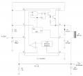
Here is a MC34063 or a AZ34063. In many ways it is much like the circuit post #3. (crutschow)

Pins-1 & 2 is the pass transistor or MOSFET.
The error amp does about the same job.
The difference; here there is an oscillator. The oscillator is gated by the error amp.
Also, there is a current limit function on pins 6 to 7.
This IC is the closest one I can think of to what you have studied. I do not use it anymore. There are better parts, but this is a good place to start.
1792896611045.png
 

crutschow

Joined Mar 14, 2008
38,909
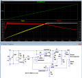
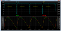
Below is a current-limit modification to the circuit, using a spare comparator in the IC package, to protect it from output short circuits:
That also makes it usable as a CC-CV battery charger.

The top plot shows the voltage (yellow trace) and current (red trace) for Rload (green trace) that goes from 1mΩ to 5Ω.
The bottom plot shows the short-circuit, peak-current limited to <2.4A for the circuit values shown.

1793111755424.png


1793111475911.png
 
Last edited:
Top