Buck Converter output not reaching reference voltages above 13V

Thread Starter

zemus_1

Joined Apr 4, 2018
20
I'm trying to step down a variable input between 15-20V to 13.6V using a buck converter. The goal is to charge a 12V battery.

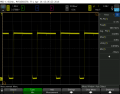
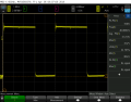
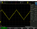
The PWM signal with the desired duty ratio is generated by comparing a triangular wave with the control output from a PI control. The attached simulation works as expected, with both resistive load and voltage load. But the breadboard testing isn't going so well.
Captura de pantalla 2018-04-04 a las 19.46.25.png Captura de pantalla 2018-04-04 a las 10.41.49.png Captura de pantalla 2018-04-04 a las 10.28.21.png
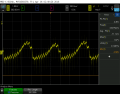
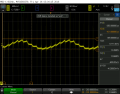
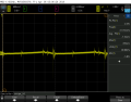
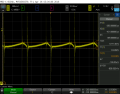
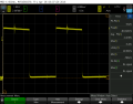
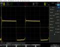
At the moment, I'm using a resistive load to see if the output is kept at the reference voltage when I vary the input voltage. For some reason, it is only able to keep the output at reference voltages below 13V. When I increase the reference above 13V, the output stays at 13V.

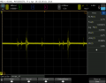
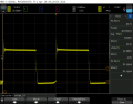
I tried connecting a voltage load to see if output was kept constant for references below 13V, but it didn't work

Could anyone give me an explanation as why the output cannot reach values for references above 13V? And what changes do I have to make if I want to connect a battery as load?

The gate driver I'm using is the IR2125 instead of the one in the simulation
 

eetech00

Joined Jun 8, 2013
3,858
HI

The LTC4446 is a boost converter not a buck converter.
According to the datasheet the max DC input is 13.5 volts.
Why do you think it will buck when its a boost converter?

eT
 

Thread Starter

zemus_1

Joined Apr 4, 2018
20
HI

The LTC4446 is a boost converter not a buck converter.
According to the datasheet the max DC input is 13.5 volts.
Why do you think it will buck when its a boost converter?

eT
The LTC4446 is the gate driver. It is used to drive the N-Mosfet in the buck converter.
 

crutschow

Joined Mar 14, 2008
34,281
Okay, I got the circuit simulating okay, as you said it did.
So, in the real circuit, measure and report the following when it's not giving the desired output:
  • The exact resistor values to get the output voltage you want (as different from the simulation).
  • Vin
  • Vout
  • Vref
  • U5 output voltage
  • U4 output voltage
  • U3 output waveform (if you have an oscilloscope)
 

Thread Starter

zemus_1

Joined Apr 4, 2018
20
Okay, I got the circuit simulating okay, as you said it did.
So, in the real circuit, measure and report the following when it's not giving the desired output:
  • The exact resistor values to get the output voltage you want (as different from the simulation).
  • Vin
  • Vout
  • Vref
  • U5 output voltage
  • U4 output voltage
  • U3 output waveform (if you have an oscilloscope)

Measurements I
----------------------
Vin= 20V
Vout≈12.9V
Vref=13.6V
Rout=330ohm

Measurements II
----------------------
Vin= 20V
Vout≈12.57V
Vref=12.6V
Rout=330ohm
 

Attachments

Last edited:

ebp

Joined Feb 8, 2018
2,332
general comments:
  • gate resistor far too high, typically no more than 20-30 ohms
  • don't know what U3_2 is, but it is a bad waveform with double transition at each rising edge
  • huge inductance
  • small output capacitance
  • appears to be incorrect frequency compensation but noise can cause what appears to be stability problems
  • large change in duty cycle shown in waveforms for very little output change
  • scope frequency and duty cycle values are wrong due to bad waveforms
  • why does low side driver have input?
 

Thread Starter

zemus_1

Joined Apr 4, 2018
20
general comments:
  • gate resistor far too high, typically no more than 20-30 ohms
  • don't know what U3_2 is, but it is a bad waveform with double transition at each rising edge
  • huge inductance
  • small output capacitance
  • appears to be incorrect frequency compensation but noise can cause what appears to be stability problems
  • large change in duty cycle shown in waveforms for very little output change
  • scope frequency and duty cycle values are wrong due to bad waveforms
  • why does low side driver have input?
Hi

  • In the breadboard testing. I used smaller gate resistors. But couldn't see any difference.
  • U3_1, U4_1, U5_1, and Vout_1 are the measurements with Vin= 20V, Vref=13.6V, and Rout=330ohm
U3_2, U4_2, U5_2, and Vout_2 are the measurements with Vin= 20V, Vref=12.6V, and Rout=330ohm
U3 is the output of the comparator. PWM signal going into the gate driver.​
  • The inductance was initially calculated for ripple of less than 1%, assuming an average current of 12A. The result was 0.75mH. Isn't it better to have bigger inductances for smaller ripple?
  • The capacitor was calculated also for a ripple of less than 1%. What kind of effects other than ripple would there be by changing capacitor and inductor values?
  • How could I fix the frequency issue?
  • Is there any way to improve quality of the signals?
  • I connected the low side just to see what I got at the output. It's not used.
 

crutschow

Joined Mar 14, 2008
34,281
Yes, the double transition at the comparator output is a no-no.
You may need to add a little positive feedback to the comparator to provide a small amount of hysteresis.
Start with about 50mV of positive feedback.

Post the voltage output at U2.
 

ebp

Joined Feb 8, 2018
2,332
Building a functional switcher is not easy. Noise is a huge problem and layout is critical.

In a typical buck converter the inductor will be chosen for peak to peak ripple of 20 to 30% of the average output current. With voltage mode control there is nothing fundamentally wrong with using a lot of inductance, but at 12 A it will require a physically large inductor. If the copper losses are to be kept reasonable, the inductor may need to be even larger to accommodate wire of sufficient diameter. To prevent core saturation the core material is likely to be expensive.

Capacitance is chosen on two fundamental criteria both related to allowable ripple: equivalent series resistance (ESR) and capacitance. The drawback of allowing larger inductor ripple is that the ESR needs to be lower and the capacitance higher to meed the voltage ripple requirement. 10 µF would allow use of just ceramic capacitors, which are in most ways much better behaved than electrolytic capacitors. At higher ripple current at moderate frequency electrolytic capacitors become necessary. Fortunately at the required voltage there are many suitable solid (polymer) electrolyte types to choose from.

The normal objective is to aim for about 45 degrees or more of phase margin when the loop crosses through 0 dB gain, preferably with a slope of -1. With voltage mode control the LC filter is 2 poles, so it has a slope of -2 (-12 dB per octave). You should be able to find lots of info on the web on error amp design. Here's on by Lloyd Dixon: http://www.ti.com/lit/ml/slup068/slup068.pdf (unfortunately, it refers to an appendix that is not included - it may be possible to find a complete Power Supply Design Seminar book that includes the appendix on the TI site - that section was included in the book for several years).

From the comparator waveform it looks like the error amplifier is commanding maximum duty cycle in the non-working case. The difference in duty cycle between the two test conditions should be very small and it is large. This suggests that the power path is unable to respond. You need to look at the FET waveform. The specified FET is grossly unsuitable for 12 ampere output.

Very large L and small C makes the response of the converter very slow to changes in load current. For battery charging this is not an issue, but it is for any sort of dynamic load requiring good response.
 

Thread Starter

zemus_1

Joined Apr 4, 2018
20
Yes, the double transition at the comparator output is a no-no.
You may need to add a little positive feedback to the comparator to provide a small amount of hysteresis.
Start with about 50mV of positive feedback.

Post the voltage output at U2.
For :
Vin=20V
Vref=12.6V
Vout≈12.56V
Rout=330ohm
I'm not sure if I did the hysteresis part correctly. I've uploaded the updated simulation
 

Attachments

Thread Starter

zemus_1

Joined Apr 4, 2018
20
From the comparator waveform it looks like the error amplifier is commanding maximum duty cycle in the non-working case. The difference in duty cycle between the two test conditions should be very small and it is large. This suggests that the power path is unable to respond. You need to look at the FET waveform. The specified FET is grossly unsuitable for 12 ampere output.
Could you explain what you mean by"maximum duty cycle in the non-working case," and "power path is unable to respond", please?

The initial design required high intensity, but now we will be working with an output of about 2-3A.

I've uploaded the signals at gate and source of the mosfet. How are these signals related to the power path you mentioned?
 

Attachments

crutschow

Joined Mar 14, 2008
34,281
I'm not sure if I did the hysteresis part correctly.
The values you selected give a hysteresis of 10k/110k * 5v = 455mV.
You probably should reduce that to closer to 100mV by changing the 100kΩ feedback resistor to about 500kΩ.

Does the circuit now work any better in outputting a higher voltage?
 

Thread Starter

zemus_1

Joined Apr 4, 2018
20
The values you selected give a hysteresis of 10k/110k * 5v = 455mV.
You probably should reduce that to closer to 100mV by changing the 100kΩ feedback resistor to about 500kΩ.

Does the circuit now work any better in outputting a higher voltage?
It's still capped at ~13V. U3 output at references above 13V is constantly changing its duty ratio.
 

ebp

Joined Feb 8, 2018
2,332
In the original set of scope images there is a very large difference in duty cycle between U3_1 and U3_2, but the output voltage is only slightly different. This should not be the case. Either there should be a large change in output voltage or a small change in duty cycle. In the case where the setpoint was 12.6 V the output was very close to setpoint and would require a duty cycle of 62.85% ignoring all sources of error and loss. In the case where the setpoint was 13.6 the output was 12.9 V, which should equate to 64.2% (for the actual output), again ignoring all sources of error and loss. But the scope image shows the duty cycle at the comparator output in the latter case to be much higher. The actual error and loss difference for the actual outputs for the two case should be nearly identical. The only way that the duty cycle can change that much without corresponding change in voltage is that something in the power path (input supply, FET, inductor, diode) is causing a problem. But again, the comparator output has that narrow extra pulse for those tests.

The second set of scope images are much better - better choice of scale makes them much easier to read. The duty cycle looks about right.

As long as the output components can handle the voltage, I suggest opening the control loop and directly controlling the duty cycle with the setpoint signal (obviously requiring some temporary rework of the circuit). This will allow you to determine if the power path is working. "U3 output at references above 13V is constantly changing its duty ratio" says to me that the loop is likely unstable. You do have three poles and one zero in the loop, and that is very unlikely to be stable. There will be a zero due to the capacitor ESR, but I'm assuming the 10 µF cap is ceramic, so the zero is probably well above the unity gain crossover frequency.
 

crutschow

Joined Mar 14, 2008
34,281
Why are you using that complex circuit instead of one of the many SMPS ICs that include the sawtooth generator and the loop compensation circuitry? :confused:
 

Thread Starter

zemus_1

Joined Apr 4, 2018
20
Why are you using that complex circuit instead of one of the many SMPS ICs that include the sawtooth generator and the loop compensation circuitry? :confused:
I thought I could apply what I've learned to make a buck converter for my design project. I couldn't just buy one.
I didn't expect it to have this much complexity, considering that the simulation worked.
Is there nothing else I can try to make this thing work?
 

Thread Starter

zemus_1

Joined Apr 4, 2018
20
In the original set of scope images there is a very large difference in duty cycle between U3_1 and U3_2, but the output voltage is only slightly different. This should not be the case. Either there should be a large change in output voltage or a small change in duty cycle. In the case where the setpoint was 12.6 V the output was very close to setpoint and would require a duty cycle of 62.85% ignoring all sources of error and loss. In the case where the setpoint was 13.6 the output was 12.9 V, which should equate to 64.2% (for the actual output), again ignoring all sources of error and loss. But the scope image shows the duty cycle at the comparator output in the latter case to be much higher. The actual error and loss difference for the actual outputs for the two case should be nearly identical. The only way that the duty cycle can change that much without corresponding change in voltage is that something in the power path (input supply, FET, inductor, diode) is causing a problem. But again, the comparator output has that narrow extra pulse for those tests.

The second set of scope images are much better - better choice of scale makes them much easier to read. The duty cycle looks about right.

As long as the output components can handle the voltage, I suggest opening the control loop and directly controlling the duty cycle with the setpoint signal (obviously requiring some temporary rework of the circuit). This will allow you to determine if the power path is working. "U3 output at references above 13V is constantly changing its duty ratio" says to me that the loop is likely unstable. You do have three poles and one zero in the loop, and that is very unlikely to be stable. There will be a zero due to the capacitor ESR, but I'm assuming the 10 µF cap is ceramic, so the zero is probably well above the unity gain crossover frequency.
I'm confused. If the system is unstable, shouldn't it be unstable no matter what reference voltage I use? Why is that it seems to work for references below 13?
 
Top