Buck converter control using an op amp instability simulation using Plecs

Thread Starter

AMANORA

Joined Sep 21, 2021
9
Good morning/ Evening. I am trying to design a buck converter. My requirments is that the closed loop output impedance is less than 0.2 across all frequencies till 20kHz.
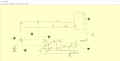
So I designed everything on paper, just couldnt asses the closed loop output impedance. Trying now to simulate the whole converter with the feedback loop to assess my design. I added a PID and chose a phase margin of 45 degree, a gain of about 23 at10kHz which is the closed loop crossover frequency. Also designed an inverted zero at 1kHz.
The output of the pid is as in the ss downards with a gain of about 29db and a phase margin of 40degree which is close to what I designed.
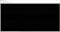
My input voltage is 100, the output voltage is also 100. It;s like there is no switching taking place.
I looked at the time domain signal coming of the PID and I found that the error is very much greater than one which makes the duty cycle equal to one.
I would really appreciate any help. I have been stuck at this for three weeks now, I wish to move onto practical stuff but I am just unable since my simulations are shit to say the least lol.
 

Attachments

Papabravo

Joined Feb 24, 2006
21,159
I would backup a bit and build an unregulated buck converter with a fixed duty cycle. The output will have an average DC value close to the intended design value with some ripple. Take that working unregulated DC-DC converter and close the the loop to see the improvements. Like this for example.

1634665535280.png

I'm curious about why there are no component values on your schematic. Can you enlighten us?
 

Ian0

Joined Aug 7, 2020
9,671
Your design seems to be missing a high-side gate driver - you have a common-drain connected N-channel MOSFET. The gate voltage will have to swing from zero to 110V, and a comparator isn't going to do that for you.
This is an excellent article on compensating the feedback loop.
 

Thread Starter

AMANORA

Joined Sep 21, 2021
9
I would backup a bit and build an unregulated buck converter with a fixed duty cycle. The output will have an average DC value close to the intended design value with some ripple. Take that working unregulated DC-DC converter and close the the loop to see the improvements. Like this for example.

View attachment 250645

I'm curious about why there are no component values on your schematic. Can you enlighten us?
Hi, I made sure that the system is stable with the a fixed duty cycle which is 0.5 .
I will upload a ss with the values of the components right away.
 

Thread Starter

AMANORA

Joined Sep 21, 2021
9
I would backup a bit and build an unregulated buck converter with a fixed duty cycle. The output will have an average DC value close to the intended design value with some ripple. Take that working unregulated DC-DC converter and close the the loop to see the improvements. Like this for example.

View attachment 250645

I'm curious about why there are no component values on your schematic. Can you enlighten us?
 

Attachments

Thread Starter

AMANORA

Joined Sep 21, 2021
9
Your design seems to be missing a high-side gate driver - you have a common-drain connected N-channel MOSFET. The gate voltage will have to swing from zero to 110V, and a comparator isn't going to do that for you.
This is an excellent article on compensating the feedback loop.
I am reading the article as we speak. But I think this is not the case since the converter is working and behaving well without the feedback loop/ open loop mode.
 

Papabravo

Joined Feb 24, 2006
21,159
You are still trying to drive a high side P-channel FET from a comparator. What does the signal on the gate look like does it swing between 0 an 100 Volts? If so tha is one heckof a comparator.
 

Thread Starter

AMANORA

Joined Sep 21, 2021
9
You are still trying to drive a high side P-channel FET from a comparator. What does the signal on the gate look like does it swing between 0 an 100 Volts? If so tha is one heckof a comparator.
The comparator output voltage is 1 volt. Which really explains that there is no switching going on. I believe the main issue is the signal coming out of the PID controller. The time domain of it is ramping instead of oscillating around a fixed point ?. What is driving me insane is that the small signal model of it is somewhat accurate to my analytical design. I just dont understand what is happening.
 

Papabravo

Joined Feb 24, 2006
21,159
First step is to identify the source terminal of the P-channel FET. It should be the terminal connected to the +100V input. When the voltage on the GATE is EQUAL TO the voltage on the SOURCE, the FET is OFF. When the voltage on the GATE is lower than the voltage on the SOURCE the FET is ON. How much lower depends on the FET. It does not need to go all the way to ground. The rds(ON) and the Vds of the FET can be found in the datasheet.

I also question the notion that a buck converter should have the same output voltage as input voltage. There are DC-DC converter technologies where this is possible, but a buck converter is not one of them.

Recommendation: If you are confused about what is going on and why a textbook on Switch Mode Power Supplies might be a useful addition to your library.
 
Top