Facebook
 Google
 GitHub
 Linkedin
I don't mind, use either. Would like to see the results of the tests. I'm going to be laying out the PCB for my version soon.Want your real name on the PCB?
I've finished it. Now for a breather, and I'll start the first tests.
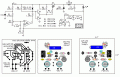
Buck converter based LED power supply
- Thread starter tom66
- Start date