BJT Model, Thoery, Usage, etc;

MrChips

Joined Oct 2, 2009
35,120
If R is constant, V and I are interchangeable, V = IR.
Hence "current amplifier" vs "voltage amplifier" is simply semantics.

A BJT is a relatively low-impedance device, hence one considers it a current amplifer,
whereas a triode or FET is a high-impedance device, hence we think in terms of a voltage amplifier.
 

t_n_k

Joined Mar 6, 2009
5,455
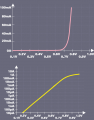
One of the most interesting things I have done is to graph Amps collector versus Volts base to emitter, Ic/Vbe

The answer was a straight line on log-log graph paper! For a 2N4250A transistor at room temperature,
.24 volts, Vbe allowed 1 nanoamp of collector current
.42 Vbe allowed 1 ua
.60 Vbe allowed 1ma

From this, I decided that an equation for Ic/Vbe can be derived, and that for every 60mv Vbe, Ic increased by a factor of 10.
I'm convinced this is a contrived "experiment".

It is simply a case of stating particular solutions for the equation

\(I_C=I_s e^{ \( \frac{V_{BE}}{0.026} \)}\)

Where Is=1E-13 A and the 0.026V is the value typically quoted as the thermal voltage at room temp.

Was it really data for a 2N4250A? Or were you simply having some fun at our collective expense?;)
 

#12

Joined Nov 30, 2010
18,224
Thank you! I am flattered that you think a simple experiment that can be done with one transistor and 2 meters seems so incredible.

Fluke 27 meter with 10M input impedance, 1% guarantee, set on the millivot scale with a resolution of .1 millivolt and placed in series with the collector. .1 millivolt across 10 megs = 10 picoamps. If I were to claim I measured a nanoamp, that would be 100 times the lowest resolution of the meter, and that is what I call accurate enough to call a nanoamp.

This measurement method has been discussed on this forum before and one of the members published it in a book he was writing, after verification, of course.

ps, where did you get that formula? When I use the data points to try to make an equation, there is no e in it. However, I did send the data to a math major friend of mine in an email today to see what he comes up with, given only the datapoints and no education in electronics. I'll bet he comes up with an equation that lacks both the e and the .026
 

t_n_k

Joined Mar 6, 2009
5,455
The equation is based on the Ebers-Moll model. The thermal voltage is more close to 0.02606 V.
Apologies for thinking you were being a practical joker. I was amazed at the 'accuracy' of the fit.
 
Last edited:

MrChips

Joined Oct 2, 2009
35,120
The equation is based on the Ebers-Moll model. The thermal voltage is more close to 0.02606 V.
Apologies for thinking you were being a practical joker. I was amazed at the 'accuracy' of the fit.
There are only three data points and hence not enough to be convincing.

You can always fit a straight line to two data points with a goodness of fit equal to 1.0.

Since the Ebers-Moll model is an exponential function, you can have a large deviation of the third point without noticing it.

For example, at Vbe = 0.60V, Ic can be anything between 0.5mA and 2mA and still get a reasonably good fit.
 

#12

Joined Nov 30, 2010
18,224
About the accuracy...I did ignore the third and foutrh digits on the Vbe meter and the .6 volt reading was really .62 but I truncated that for the benefit of the person I was talking to. I have a feeling that if I told Austin Clark the last measurement was off by 3.3% he would poke holes in me AND Ebers-Moll, or at least demand several explanations.

I am weak enough in math that I see only powers of ten, so I expect an equation that will be in the form of log base 10. My first attempt came up with Vbe = .065 log (5e12 x Ic). That's why I have a math major to help me (and he has an electronics guy to help him).

I actually did the experiment, just because so many people have said, "about .6 volts to turn the transistor on" and real world measurements have told me that isn't exactly true. I was surprised to find the results are a straight line on log/log paper. That completely shoots down the idea that some particular voltage is required to activate a bjt transistor.
 

Jony130

Joined Feb 17, 2009
5,599
I actually did the experiment, just because so many people have said, "about .6 volts to turn the transistor on" and real world measurements have told me that isn't exactly true. I was surprised to find the results are a straight line on log/log paper. That completely shoots down the idea that some particular voltage is required to activate a bjt transistor.
That should be no surprise. It's well known fact that "diode" exponential curve straightens out when we use a log/log plot.
And from the practical point of view we assume that BJT is ON when Vbe > 0.5V.
 

Attachments

MrChips

Joined Oct 2, 2009
35,120
That should be no surprise. It's well known fact that "diode" exponential curve straightens out when we use a log/log plot.
And from the practical point of view we assume that BJT is ON when Vbe > 0.5V.
That should be a semi-log plot, with log on the current scale (Y-axis) and linear on the voltage (X-axis).

A log-log plot appears to be a straight line because the voltage range from .24v to .60V is not even a decade.
 

WBahn

Joined Mar 31, 2012
33,133
I've skimmed through the entire thread, but have not read every post in detail. I'll just throw out a few points and hopefully I'm adding stuff and not just repeating what others have already said.

Point #1: The question of whether a transistor is best described as a switch, a current amplifier, a current controlled resistor, a (several other possibilities) has no hard answer. The best description is the one that is most applicable to the intended application and the performance specs that must be met. Yes, in theory, you could "simply" take the most complete model for the transistor that you can find and use it for every design you ever do, but doing so actually makes you a monkey and not an engineer. This is especially true given that modern transistor models are extremely complex in order to model increasingly pronounced high-order effects. Some of the FET models we use in designing simulations are subcircuits containing over 300 components. That level of complexity is necessary to obtain reasonable accuracy when designing analog ICs with deep sub-micron processes. Does that mean that we should use such complex models with designing a simple logic circuit or turning on an LED? Of course not, unless you are a monkey. Part of being an engineer is learning when and how to use the different models and, in general, abide by the mantra that if the answer is "good enough", then it is "good enough" and using a more details model or spending a lot of time and effort to get better performance is a waste of your customer's money.

Point #2: Quite a bit seems to have been said regarding the often stated "turn on voltage of about 0.6V" for a transistor and much of it seems to have ingored the "about" portion of that phrase. Anyone that tries to claim that there is a fixed voltage at which a silicon diode or BJT transistor begins to conduct and that it doesn't conduct at all below that point and conducts freely over that point is making a gross oversimplification of reality - but, by the same token, that gross oversimplication is more than adequate for many, many design and analysis problems.

Most circuits are going to be designed to operate with BJT currents ranging over a couple orders of magnitude and few will be designed to operate over more than four orders of magnitude. At room temperature, the BJT current will change by an order of magnitude for every 60mV change in base-emitter voltage, so two orders of magnitude is only +/-60mV from some nominal voltage. For most devices, that nominal voltage is parked somewhere in the 0.5V to 0.7V range by the device designer. If, for your intended application, the difference between being 500mV and 700mV (or even widen it out a bit further and say 400mV and 800mV) makes a significant difference, then by all means use a more detailed model. Otherwise, use the nominal voltage and accept that there is some error but that the error is within acceptably limits. Many people use 500mV for power transistors and 700mV for small signal transistors and 600mV for stuff inbetween. That rule of thumb is a reflection of how many devices are designed given the range of intended applications for that device.

Point #3: There was some discussion of how much the collector current changes by if the collector voltage is changed while the base current is kept constant. I saw a few people say that the collector current is independent of the collector-emitter voltage (provided the device remains in the active region). This, of course, is only an approximation but, again, an approximation that is "good enough" for a huge fraction of design problems. In reality, a much better approximation is that the collector current increases as the collector-emitter voltage changes. A very good (but not perfect) model for this change is that the slope of the Ic vs Vce curves in the linear region project back to a single voltage at zero current that is known as the Early voltage (since the point on the graph is a negative votlage, the Early voltage is the negative of that voltage so that we can work with positive parameters as much as possible to minimize stupid math mistakes). The Early voltage is typically between about 10V and 200V (the bigger the better).

Point #3: For most applications that can't use a nice, simple linear model in which the collector current is some multiple of the base current and that the base-emitter voltage is fixed at around 0.6V, it is sufficient to use superposition to spilt the design into a large signal bias circuit and a small signal circuit. For many of those applications, it is sufficient to use a voltage-controlled current source model for the transistor and, as the application warrants, incorporate the Early voltage and, if the frequency of operation is high enough, the effective capacitances between each of the three nodes. If that still isn't good enough, then most applications should move toward simulation-based designs using transistor models that are of adequate fidelity for the transistors actually used (i.e., at this point, you have probably moved well beyond what a generic transistor model can provide).
 

Thread Starter

Austin Clark

Joined Dec 28, 2011
412
I've skimmed through the entire thread, but have not read every post in detail. I'll just throw out a few points and hopefully I'm adding stuff and not just repeating what others have already said.

Point #1: The question of whether a transistor is best described as a switch, a current amplifier, a current controlled resistor, a (several other possibilities) has no hard answer. The best description is the one that is most applicable to the intended application and the performance specs that must be met. Yes, in theory, you could "simply" take the most complete model for the transistor that you can find and use it for every design you ever do, but doing so actually makes you a monkey and not an engineer. This is especially true given that modern transistor models are extremely complex in order to model increasingly pronounced high-order effects. Some of the FET models we use in designing simulations are subcircuits containing over 300 components. That level of complexity is necessary to obtain reasonable accuracy when designing analog ICs with deep sub-micron processes. Does that mean that we should use such complex models with designing a simple logic circuit or turning on an LED? Of course not, unless you are a monkey. Part of being an engineer is learning when and how to use the different models and, in general, abide by the mantra that if the answer is "good enough", then it is "good enough" and using a more details model or spending a lot of time and effort to get better performance is a waste of your customer's money.

Point #2: Quite a bit seems to have been said regarding the often stated "turn on voltage of about 0.6V" for a transistor and much of it seems to have ingored the "about" portion of that phrase. Anyone that tries to claim that there is a fixed voltage at which a silicon diode or BJT transistor begins to conduct and that it doesn't conduct at all below that point and conducts freely over that point is making a gross oversimplification of reality - but, by the same token, that gross oversimplication is more than adequate for many, many design and analysis problems.

Most circuits are going to be designed to operate with BJT currents ranging over a couple orders of magnitude and few will be designed to operate over more than four orders of magnitude. At room temperature, the BJT current will change by an order of magnitude for every 60mV change in base-emitter voltage, so two orders of magnitude is only +/-60mV from some nominal voltage. For most devices, that nominal voltage is parked somewhere in the 0.5V to 0.7V range by the device designer. If, for your intended application, the difference between being 500mV and 700mV (or even widen it out a bit further and say 400mV and 800mV) makes a significant difference, then by all means use a more detailed model. Otherwise, use the nominal voltage and accept that there is some error but that the error is within acceptably limits. Many people use 500mV for power transistors and 700mV for small signal transistors and 600mV for stuff inbetween. That rule of thumb is a reflection of how many devices are designed given the range of intended applications for that device.

Point #3: There was some discussion of how much the collector current changes by if the collector voltage is changed while the base current is kept constant. I saw a few people say that the collector current is independent of the collector-emitter voltage (provided the device remains in the active region). This, of course, is only an approximation but, again, an approximation that is "good enough" for a huge fraction of design problems. In reality, a much better approximation is that the collector current increases as the collector-emitter voltage changes. A very good (but not perfect) model for this change is that the slope of the Ic vs Vce curves in the linear region project back to a single voltage at zero current that is known as the Early voltage (since the point on the graph is a negative votlage, the Early voltage is the negative of that voltage so that we can work with positive parameters as much as possible to minimize stupid math mistakes). The Early voltage is typically between about 10V and 200V (the bigger the better).

Point #3: For most applications that can't use a nice, simple linear model in which the collector current is some multiple of the base current and that the base-emitter voltage is fixed at around 0.6V, it is sufficient to use superposition to spilt the design into a large signal bias circuit and a small signal circuit. For many of those applications, it is sufficient to use a voltage-controlled current source model for the transistor and, as the application warrants, incorporate the Early voltage and, if the frequency of operation is high enough, the effective capacitances between each of the three nodes. If that still isn't good enough, then most applications should move toward simulation-based designs using transistor models that are of adequate fidelity for the transistors actually used (i.e., at this point, you have probably moved well beyond what a generic transistor model can provide).
Maybe I'm just overestimating the % error that will arise in using approximate models. For example, if you were to use a voltage divider to supply a specific voltage to the base of a BJT, wouldn't you have to take into account the voltage drop that will occur when the base conducts some current? And would it not take some fairly complicated math to solve for that? Beings that you'd have to find a point in which the base's equivalent resistance will cause the input voltage to cause itself to be at that equivalent resistance. (if that makes any sense, kinda like finding the voltage drop across a diode in a diode-resistor series circuit, just slightly more complicated).

I don't need PERFECT models for everything, for example, I don't assume resistors to have capacitance, reactance, inductance, to be thermally affected, or vary in respect to humidity, voltage, etc; etc;
Realistically, given a better model you can only eventually develop more accurate and more efficient circuits, and with modern computers I don't see it being too difficult to plug in parameters and computer automatically a optimized circuit, or at least optimized subcircuits.

Also, it just sorta bugs me not having a clue how approximate these models are in specific cases, I'd at least like to calculate once-and-for-all how inaccurate the estimates will be to both put my mind at rest when going ahead and using the approximate models and to let me know when it's reasonable to use the more complete models.

Overall, I'm just complicated like that. :)
 

Thread Starter

Austin Clark

Joined Dec 28, 2011
412
Ok, I've been experimenting with a java circuit simulator, working with the math, etc; and I THINK I've come up with a fairly accurate model to use in my digital circuit design process. One in which I SHOULD be able to, hopefully, better predict and refine my results.

Please tell me if this model is correct in theory, and if not where have I made a mistake and how do I fix it?

**************************************

IF BEi*β > Vs/R1
Where R1 is the resistor value behind the collector.
the equivalent circuit output is essentially a direct connection to ground.
In other words, when the transistor tries to conduct more through the Collector-Emitter junction than the resistor will allow, the output is a direct connection to ground, where the output is at the collector, and the energy dissipated would be:
BEi*BEv + Vs^2/R1

ELSE the equivalent circuit output (again the output being at the collector) is a voltage divider where the source voltage is just Vs, the first resistor is just R1, and the second resistor (in which the output will be behind) will have a value of:
Vs/(BEi*β) - R1
and the energy dissipated would be:
BEi*BEv + BEi*Vs*β

:D

I came to this model assuming that the transistor will adjust it's resistance to ensure that it will conduct BEi*β across the CE junction, but it cannot reduce its resistance below 0 (obviously), so when it can't do that the current through the CE junction is just whatever the circuit leading to the collector will allow.
I know you all were trying to explain something like that to me earlier, but it just didn't click until I experimented with the simulator, and just did my own thing.

The only problem with this model is that calculating the current through the base can be troublesome, and there's no easy-yet-close-to-ideal model for it that I've come up with thus far.
 

WBahn

Joined Mar 31, 2012
33,133
Because the collector current is such a strong function of base-emitter voltage, few circuits attempt to apply a base-emitter voltage directly. If nothing else, the value of the saturation current is seldom well characterized and varies from transistor to transistor and with temperature and other things.

Instead, the circuit is designed so that it will automatically settle at the correct Vbe as a result of negative feedback in the circuit's normal operation.

For instance, consider a circuit in which you have an NPN transistor in which the base is connected directly to a low-impedance signal source (say a 9V battery) and the emitter is connected to ground (i.e., 0V)through a 10kΩ resistor and the collector is connected to a +15V supply through a 1.8kΩ resistor. What is the voltage at the collector?

First, let's use an extremely simply transistor model in which the base-emitter voltage is 0.6V and assume infinite beta. In that case, the emitter voltage is at 8.4V (the fixed 9V at the base minus the 0.6V drop for Vbe). This makes the emitter current 8.4V/10kΩ which is 0.84mA. Since we are assuming infinite beta, this is also the collector current and, therefore, the collector voltage is 15V-0.84mA*1.8kΩ, which is 13.49V.

At this point, we can check whether the collector-emitter voltage, Vce, is greater than the saturation voltage, which is typically about 0.25V. In this case, we have Vce = 5.09V, so we know that the transistor is comfortably in the linear region.

Our negative feedback comes from the emitter resistor because if we increase the base voltage by, say, 60mV, then that would try to increase the collector current by an order of magnitude. However, as soon as the collector current starts to increase, the emitter current increases and, hence, the voltage at the emitter increases due to the emitter resistor. Thus, the current doesn't increase by an order of magnitude, but rather only by about 60mV/Re, which is usually going to be pretty small. Similarly, a beta of 25 compared to a beta of 100 will only result in about a 3% change in the collector current because the base current goes from being about 4% of the emitter current to only being about 1% of the emitter current.

The best way to learn how to make decisions regarding when to use what models is to design lots of circuits of various types and try out the different models and see whether they made a significant difference. It's not as bad as it sounds. Very quickly you will get a feel for when simple models are sufficient and when more complex models are needed. Furthermore, you will learn how to start recognizing when a circuit is likely to be too sensitive to device or model parameters, which usually means that it is time to use a different circuit, or at least modify the circuit to reduce the sensitivity.
 

studiot

Joined Nov 9, 2007
4,998
calculating the current through the base can be troublesome
Did you stop the wonder if that's why nobody uses this type of circuit configuration?

Transistors have a wide spread of parameter variation. Fets even wider.

A good circuit is one that is insensitive to this variation. In other words designed so that we can take 10 random transistors out of a box of 1000, plug them into the same circuit and achieve identical action.

Worse the parameters for an individual transistor will vary with collector current and temperature. We need our circuit to be insensitive to these variations as well.

I pointed you at two ports for a good reason. Do you wish to explore them further?
 

Thread Starter

Austin Clark

Joined Dec 28, 2011
412
Did you stop the wonder if that's why nobody uses this type of circuit configuration?

Transistors have a wide spread of parameter variation. Fets even wider.

A good circuit is one that is insensitive to this variation. In other words designed so that we can take 10 random transistors out of a box of 1000, plug them into the same circuit and achieve identical action.

Worse the parameters for an individual transistor will vary with collector current and temperature. We need our circuit to be insensitive to these variations as well.

I pointed you at two ports for a good reason. Do you wish to explore them further?
http://i12.photobucket.com/albums/a220/saladsamurai/Screenshot2011-02-05at101244PM.png

Many logic gates seem to use the configuration I was referring to.

Yes, I am interested in two ports. Not sure where to begin on that front though.

Regardless, I found out that the collector voltage affects conduction in the BE. What's the equation to find the BE current?
 

Jony130

Joined Feb 17, 2009
5,599
The base current is always equal to :

Ib = (Vin - Vbe)/RB


but what about the collector current?
First we usually assume that bjt work in the active region.
So the collect current is equal

Ic = β * Ib

And collector-emitter voltage

Vce = Vcc - (Rc * Ic)

And if

Ic > Vcc/Rc ----> (β * Ib) > (Vcc/Rc) the BJT is in saturation region.

And Ic = β * Ib don't hold anymore.

So if we design BJT to work as a switch we need ensure the BJT will be in the saturation region.

So we have a two equations

Ib = (Vin - Vbe)/Rb (1)

Vce = Vcc - (Rc * Ic) (2)

Vce = Vcc - Ic*Rc = Vcc - β*Ib*Rc =Vcc - β*(Vin - Vbe)/Rb*Rc = Vcc - β*Rc/Rb * (Vin - Vbe) --> Solve for Rb

Rb = (Vin - Vbe)/(Vcc - Vce) *β * Rc

\(Rb \leq \frac{(Vin - Vbe)}{(Vcc - Vcesat)} * \frac{\beta{min}}{K} *Rc\)

where

K is a overdrive coefficient ( typical from 2 to 5)

Or sometimes we use a simpler rule
We selected Rc and Rb that we ensure

Ic/Ib = 50...10

Rb = (Vin_min - Vbe)/ ( (Vcc/Rc)/10)
 
Last edited:

Thread Starter

Austin Clark

Joined Dec 28, 2011
412
The base current is always equal to :

Ib = (Vin - Vbe)/RB


but what about the collector current?
First we usually assume that bjt work in the active region.
So the collect current is equal

Ic = β * Ib

And collector-emitter voltage

Vce = Vcc - (Rc * Ic)

And if

Ic > Vcc/Rc ----> (β * Ib) > (Vcc/Rc) the BJT is in saturation region.

And Ic = β * Ib don't hold anymore.

So if we design BJT to work as a switch we need ensure the BJT will be in the saturation region.

So we have a two equations

Ib = (Vin - Vbe)/Rb (1)

Vce = Vcc - (Rc * Ic) (2)

Vce = Vcc - Ic*Rc = Vcc - β*Ib*Rc =Vcc - β*(Vin - Vbe)/Rb*Rc = Vcc - β*Rc/Rb * (Vin - Vbe) --> Solve for Rb

Rb = (Vin - Vbe)/(Vcc - Vce) *β * Rc

\(Rb \leq \frac{(Vin - Vbe)}{(Vcc - Vcesat)} * \frac{\beta{min}}{K} *Rc\)

where

K is a overdrive coefficient ( typical from 2 to 5)

Or sometimes we use a simpler rule
We selected Rc and Rb that we ensure

Ic/Ib = 50...10

Rb = (Vin_min - Vbe)/ ( (Vcc/Rc)/10)
Heck yes, thank you so much for that.

Only two more questions! XD

K is basically the "buffer" correct? Basically, if it's 2, you're going to make it so that the maximum Ice is 1/2 β*Ibe? To ensure that the transistor remains in saturation? (close to or at 0 ohms resistance across it's CE junction).

Also, I'm still having trouble understanding Ibe.
You said it's always Ib = (Vin - Vbe)/Rb, which makes sense, but to how do you know Vbe? I found that Vc actually affects Ib, can you explain this?
 
Top