BJT - CE Amplifier Design simulation & Calculation

Thread Starter

mishra87

Joined Jan 17, 2016
1,063
Hello Everyone !!!

Hope you are doing well.

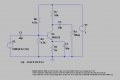
I have drawn a common emitter amplifier using BJT.
I have assume some values in the circuit and have not done any paper calculation.
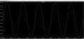
Simulation files are attached herewith ( Circuit, input & Output)

I do not know how & where to start with.

Could anybody guide to design a amplifier.

1. What is design specification for design a amplifier.
2. What all parameters needs to take in consideration while designing amplifier.
3. How to load line analysis and set operating point of amplifier.
4. How to define gain of a amplifier.
5. What should be frequency response of a amplifier.
6. How to calculate the component used in schematic.
7. How to calculate coupling in schematic.
8. Input is 300mV and why output is 4V.
9. What is role of current and voltage gain in the circuit.

My intention of starting this is to understand about BJT as a amplifier and able to do black box calculation before doing simulation or building a circuit in PCB.

Please consider me beginner while explaining the schematic.

Thanks in Advance. !!!
 

Attachments

Jony130

Joined Feb 17, 2009
5,598
1. What is design specification for design a amplifier.
The basic one are:
Desired voltage gain/current gain/power gain.
Desired input and output resistance, you need to know what's driving the circuit (what is the source of signals), what it a load of our amplifier.
Desired frequency response.
And there's much more, of course, but context matters.

What all parameters needs to take in consideration while designing amplifier.
It up to the designer to decide what parameter he thinks are important for a given circuit.
For example, sometimes, the input resistance is not so important becouse we know that driving circuit has low impedance. So we do not care about Rin much.

4. How to define gain of a amplifier.
The voltage gain is Av = Vout/Vin
The Current gain Ai =Iout/Iin
Power gain Ap = Pout/Pin
5. What should be frequency response of a amplifier.
You as a designer need to know the purpose of the amplifier you are trying to build and the input signal frequency range.

6. How to calculate the component used in schematic.
http://www.learnabout-electronics.org/Amplifiers/amplifiers21.php

. How to calculate coupling in schematic
http://www.learnabout-electronics.org/Amplifiers/amplifiers22.php
General equation:

C = 1/(2 * pi * F *R) ≈ 0.16/(F*R)

Input is 300mV and why output is 4V.
First of all, without any input signal, your BJT is in saturation. You have wrongly chosen the DC condition (quiescent point).
This is why the amplifiers leaving the saturation region for a negative half of an input signal.
 

Zeeus

Joined Apr 17, 2019
616
First of all, without any input signal, your BJT is in saturation. You have wrongly chosen the DC condition (quiescent point).
This is why the amplifiers leaving the saturation region for a negative half of an input signal.
= change Rc...Emitter current is about 1.8mA so 1.8 * Rc = 2500
 

hobbyist

Joined Aug 10, 2008
892
Lets just take a look at your circuit and see if it will work as an amplifier.

This will get you some practice in designing transistor amplifiers, by analysing
these kind of problems systematically.

I'm assuming you are well grounded in ohms law and voltage dividers etc.

look at your circuit and determine where you can calculate a voltage drop.

Can you imediately calculate the voltage at the emitter of the stage?
If not why not?

How about the collector terminal can you do an immediate calculation of voltage there, again if not why not?

How about the base terminal, can you do an immediate calculation there?

At the base terminal you have a voltage divider across the supply line.

That may be a good place to start your analysis.

Using the voltage divider equation shows that half the supply is at the base terminal, would you agree?

When doing first order analysis, you need to make educated assumptions, such as the voltage divider is not sinking current into the transistor base terminal. Also an assumption that the base emitter voltage potential (vbe) is around 0.65V or so to be operating. so with those assumptions you can calculate what the emitter voltage should be around
by using ohms law rearranged in several ways.

So taking the voltage at the base terminal to be around 2.5V would than mean you have to
drop another 0.65V to get the emitter voltage, so {(2.5V - 0.65V)~=1.85V.} rearranging ohms law equation you can solve for current through the emitter resistor, {(1.85V / 1K ohms)~=1.85mA} Now rearanging ohms law again you can now solve for the voltage drop across the collector resistor, {(1.85 mA * 10K ohms)~=18.5V} So that means your transistor has no voltage drop acrosss it, which as someone pointed out it is in saturation.

Now you know it is impossible for that much voltage to be dropped across the collector
resistor, but you are able to analyse that the transistor is saturated by this bias configuration.

How to remedy it.
Start your design by assuming a voltage drop across the collector resistor to be around half
the supply voltage. That would then leave half the supply voltage to be dropped across both
the transistor and emitter resistor. So if you have determined that your collector resistor needs to be 10K ohms, than start there and calculate the current flowing through it if half the supply is dropped across it. {(2.5V / 10K ohms)=250uA (IC)}

Now it looks like you are trying to get a DC gain of around 10 for this stage, so keeping your 1K value as the emitter resistor, than calculate your voltage drop across the emitter resistor {(250uA * 1K ohms)=250mV (VRE)}

Now You can solve for your base voltage by adding to the emitter voltage (0.65V) so {(0.25V + 0.65V)=0.85V (VB)}

Now it is good practice to make the current flowing in the base voltage divider to be at least
ten times greater than the emitter current, so as to not load down the divider voltage.

So {(10 * 250uA)=2.5mA} now you can calculate first order approximation the base bias resistors by taking your base voltage divided by the new current value you just calculated.
{(0.85V / 2.5mA)=340 ohms. (R2)

Now to solve first order approximation the pull up base bias resistor, take the supply voltage and subtract from it the base voltage than divide into it the divider current.
{(5V - 0.85V)=4.15V and (4.15V / 2.5mA)~=1.6K ohms (RB).

Now build it and test it to see how it operates.
Use resistors of closest practical values.

Now as you do an analysis of this design you will see several short comings about it.

First off as yu were doing your calculations the collector current is fairly low value.

But that is not as important as your emitter voltage versus the (Vbe) value.(0.65V)

You should always design the emitter voltage to be at the very least the same value as Vbe but much greater is more desirable. The reason is that any change in Vbe will have a significantly effect on the emitter current thus causing collector voltage to be unstable, because the Vbe (0.65V) is an unstable value as temperature at the transistor junction changes, so you should always design your emitter voltage to be around 1 v or more depending on circuit parameters.

Now that yu have that established you can rework your design to get a more stable stage.
For instance if you choose to make the emitter voltage 1V than emitter resistor (R1) will be around 4K ohms now your DC gain has gone down considerably but you can recover some AC gain with a proper emitter capacitor, but now your emitter voltage is more fixed against temperture changes at the base emitter junction where (Vbe changes).

Now you need to rework values for you base bias resistor divider network.

Your new base voltage (VB) will be around 1.65V and {(1.65V / 2.5mA)~=660 ohms (R2) And again resolving for (Rb) gives {(5V - 1.65V)=3.35V and (3.35V / 2.5mA)=1.3K ohms (Rb) Use resistors of closest practical values.

As you will see your gain will be much lower do to the (Rc / R1) value, but you can increase AC signal gain by adding your emitter bypass cap into the emitter lead as you have shown on your schematic.

This should help you get started in designing bias networks for CE transistor amps.
 

Audioguru

Joined Dec 20, 2007
11,248
The output image has a dark blue rectangular-wave on a black background that was invisible until I closed the blinds in my computer room.
The resistor values were selected at random instead of being properly calculated.
 
Top