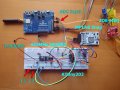
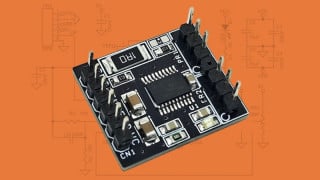
Just capacitor voltage divider with C1=6.8nF and C2=2.2nF. Add LMC6482 as voltage follower (powered by 3.3V) and that is. For my project I will do single ADC Vbat measurement each hour.
hi K,
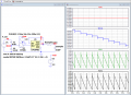
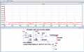
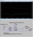
This is what LTSpice shows using those components.
Two plots, set for 100 seconds run, sampling plot during the last 1 Second
First plot with Vbty = 4.12V and the 2nd plot Vbty 3.3v
Assuming Vref =3.3v and that you are sampling at the lowest voltage point
Using your figures of 4.12v== 0xD6 [214] & 3.3v = = 0XA2 [162]
Thats is:
3.3v(214/255) = 2.77v [ the lowest value on the plotted waveform shows 2.76v]
&
3.3v(162/255)= 2.09v [ the lowest value on the plotted waveform shows 2.26v]
So I would say the LTSpice output is close to the actual circuit
E
hi K,
It will be interesting to see the performance in the final build.
I expect there will a minor change in the ADC values due to tidy up of those long wiring capacitance values.
E
Hi ericgibbs,
Don't worry. I will use the 0201 packages for components, the PCB will be about 8 x 35 mm to fit into cat's collar for their GPS/LoRa tracking.
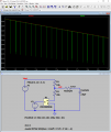
So Vdivo falls by about 100uV per sample, and at 1 sample per hour that's an error of 2.4mV per day, which will accumulate to be quite significant over a few days.
Then you change from breadboard to pcb using 0201 components, with a creepage distance of about 0.4mm instead of 15mm, and the possibility of flux residues under the components, so about 40 times the surface leakage currents.
Good luck!
Hi Ian0,
Instead of simulations, try measuring voltages on real components. I think there will be almost no current leakage when using a MAX40023 Op Amp with a Rin of about 15TΩ. C1 and C2 will still be charged from the Vbat.
Hi ericgibbs,
Although your simulation is nice, I don't think it's correct. The voltages on C1 and C2 cannot decrease with time because both capacitors are still connected to a constant DC voltage source. The voltage on both capacitors must still equal the input voltage Vbat 4.2V or 3.3V. Although the pulse of switch S1 may cause the voltage on C2 to drop for a very short period of time, when the switch is released, C2 quickly recharges to the original value given by Vbat and the ratio of the values of the two capacitors.
Because C1 and C2 is still connected to Vbat. If there is no resistor connected in parallel to C2, the voltage at the output of C2 must be proportional to CVD (Capacitor Voltage Divider).
Unfortunately not, there is always the surface resistance of the pcb in parallel with R2, and even if there weren’t the input capacitance of U1 (about 3pF) and all the pcb parasitic capacitance gets connected across C2 every time it samples. I suspect the effect would be rather worse than @ericgibbs simulation predicts, as it does not include the parasitics.
I don't understand how the parasitic capacitance of the PCB or input capacitance of U1 during sampling can cause a permanent slow voltage drop on capacitors that are permanently connected to a "hard" voltage source.
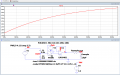
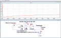
This simulation explains the CVD problem. When sampling the voltage on C2 without using an Op Amp, its voltage drops temporarily (C2 discharges see -0.4 mA), which causes it to start charging to a higher voltage C1 at the same time (C1 current is almost +1.0 mA), and then the voltage value of C2 can no longer return to its original value before S1 is switched on.
It would be interesting to simulate the minimum load of C2 using an Op Amp with a high input impedance.
The only problem is that I don't know why the Vbat voltage dropped at the same time, which should have stayed the same.
The problem with that is, when the MOSFET is OFF the full battery voltage is connected to the ADC input through the 10k resistor. Current will flow from the battery through 10k and the upper protection diode into the 3.3V supply

 Facebook
 Google
 GitHub
 Linkedin