Audio amplifier

Ian0

Joined Aug 7, 2020
13,132
Note the different values for the gate resistors, something else that was not copied over correctly.

ak
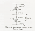
Even Hitachi aren’t consistent with that. One design has them all at 100Ω, and the other has P-channel at 220Ω and N-channel at 330Ω.
I always use a much lower value, because too high a value puts a pole inside the feedback loop, at a frequency where there is still closed-loop gain, which is not good for stability.
 

MrAl

Joined Jun 17, 2014
13,704
Here it is. There are two versions. I always thought I had two copies of the same data book, but they are actually different.
I’ve never seen the version with the cascaded JFET front end in a commercial amplifier.
It goes on to class-D designs on the next page. Let me know if you want that as well, as it’s not exactly relevant to this topic.View attachment 343350View attachment 343351View attachment 343352View attachment 343353View attachment 343354View attachment 343355View attachment 343356View attachment 343357
View attachment 343350

Thanks for the info there!

The thing that bothers me though is that the bias scheme is different for all those designs than for the one we had been considering, and that was the main question that came up in this thread by several members. I think this leads us to still be a little shy of explaining the original design.

The main concern I think is how to best drive the output stage (see attachment). V1 and V2 will be related in some way, but they can't be just anything. I do have to question if V1 is higher than V2 by 1.4 or 1.5v all the time, will the transistors be able to produce 0v output voltage (Vout) with not too much of an excess current in either the upper or lower transistor.
We could look into this in more detail.
 

Attachments

Ian0

Joined Aug 7, 2020
13,132
In the two Hitachi circuits, the MOSFETs are driven from a current-mirror-loaded long-tailed pair, so the output side is effectively driven by a constant current source. A resistor with a constant current through it is a constant voltage, so the preset gives a constant voltage bias to the two MOSFETs, so it's almost identical to the diode bias scheme.
At 0V output, there will be 1.2V across the pair of diode, with 0.6V across the Vgs of each transistor.Screenshot from 2025-03-01 08-14-03.pngScreenshot from 2025-03-01 08-14-53.pngThat would give a bias current through the FETs of around 100mA, and it is biased at about the Vgs zero temperature coefficient point so the bias stays stable with temperature.
(With two diodes, the bias will fall with temperature, due to the temperature coefficients of the diodes, so it would actually work better if the diodes were away from the heatsink)
 

MisterBill2

Joined Jan 23, 2018
27,522
IN ADDITION TO THE PREVIOUS COMMENTS, please realize that the amplifier circuit is a directly coupled amplifier, meaning that every stage affects all the other stages, and that to function correctly it must be adjusted for "perfect balance".
The whole concept of a direct coupled amplifier is based on both "perfect" components and "perfect balance", which is not likely to happen except in a perfect circuit simulator.
I would not ever suggest such a design to anybody, except as an example of what choices to avoid.
Aside from that problem, certainly the comments about the inadequate changes for using an FET output section also apply.
 

Ian0

Joined Aug 7, 2020
13,132
IN ADDITION TO THE PREVIOUS COMMENTS, please realize that the amplifier circuit is a directly coupled amplifier, meaning that every stage affects all the other stages, and that to function correctly it must be adjusted for "perfect balance".
The whole concept of a direct coupled amplifier is based on both "perfect" components and "perfect balance", which is not likely to happen except in a perfect circuit simulator.
I would not ever suggest such a design to anybody, except as an example of what choices to avoid.
Aside from that problem, certainly the comments about the inadequate changes for using an FET output section also apply.
Not true. It's a feedback amplifier, so most of it can be quite non-linear. If the error amplifier (i.e. the first long-tailed pair) has enough gain it will correct any non-linearities and DC offsets created by the rest of the circuit: distortion will be reduced by the factor of open loop gain divided by closed loop gain. Matching between components with the exception of the two transistors in the first long-tailed pair is not of great importance.
Bipolar transistors, lateral MOSFETs and vertical MOSFETs are all voltage-controlled devices. Setting the bias for a complementary emitter follower or complementary source follower is the same in all three cases, only the bias voltage is different. All three can make use of a resistor driven by a constant current source, a number of diodes, a zener or a Vbe multiplier circuit. The lateral MOSFET is the least critical as the forward transconductance is quite low, especially around the threshold voltage, and no temperature compensation is required.
The firm for which I worked produced an amplifier to an almost identical circuit in considerable quantites. It was reliable, performed well and needed no adjustments on setting up.

By the way, the feedback resistor in the simulation is wrong. It is 47Ω when it should be 47k.
 

AnalogKid

Joined Aug 1, 2013
12,130
IN ADDITION TO THE PREVIOUS COMMENTS, please realize that the amplifier circuit is a directly coupled amplifier, meaning that every stage affects all the other stages, and that to function correctly it must be adjusted for "perfect balance".
The whole concept of a direct coupled amplifier is based on both "perfect" components and "perfect balance", which is not likely to happen except in a perfect circuit simulator.
I would not ever suggest such a design to anybody, except as an example of what choices to avoid.
Aside from that problem, certainly the comments about the inadequate changes for using an FET output section also apply.
This just in: A comprehensive study of the internal circuitry of 99.999% of commercially available integrated circuit operational amplifiers and instrumentation amplifiers reveals a shocking truth - all of them are direct coupled. Note that the first direct-coupled opamp was patented in 1946, 1-1/2 years and 12 days before the invention of the transistor.

https://patents.google.com/patent/US2401779

<gasp>

ak
 
Last edited:

MisterBill2

Joined Jan 23, 2018
27,522
The internals of manufactured IC devices are controlled much better than a hobbyist built amp. And direct coupled stereo amps have a bad reputation in my area. I have seen where a failed transistor in the second stage took out the final power stage. Your results may differ. Or you may never had to troubleshoot one of them.
 

Ian0

Joined Aug 7, 2020
13,132
The internals of manufactured IC devices are controlled much better than a hobbyist built amp. And direct coupled stereo amps have a bad reputation in my area. I have seen where a failed transistor in the second stage took out the final power stage. Your results may differ. Or you may never had to troubleshoot one of them.
Amplifiers that achieve sub 10ppm distortion are generally made from discrete transistors.
I've never found troubleshooting a big problem. After checking the ones that the customer is most likely to blow up - the output stage from overloading it, or the input stage from connecting the mains to the input jack (or whatever they manage to connect in there, sometimes I wonder) , if you haven't found the dead one, just go around all the transistors until you find one where the value of Vce isn't what it should be for the value of Vbe.
 

MrAl

Joined Jun 17, 2014
13,704
Hi,

I have to agree that feedback changes things a lot and can correct for a lot of issues. That's one of the reasons negative feedback came about.
Unfortunately I have not had a chance to look into the current circuit enough yet. I have some computer issues I am working out. What pain in the neck Windows can be sometimes, and I made the big mistake of updated to version 24H2 of Win11. Never again until ALL the bugs are corrected.
 

MrAl

Joined Jun 17, 2014
13,704
It the only sort I’ve ever worked with, so I’ve learned how to deal with them!
When I first learned about negative feedback I was amazed how handy it could be to correct errors. Kudos to Mr. N. Feedback wherever you are :)
 

pe1hmm

Joined Jul 8, 2020
2
In the initial message, joni.vanderhaeghe mentioned that only the VCC-connected FETs became hot. Apart from all mentioned updates, hints and tips, keep in mind that the current for making high FET temperatures also has to go somewhere. That can only be through the VEE supply (already shortened FETs?) and/or your woofer!
 

MisterBill2

Joined Jan 23, 2018
27,522
Certainly negative feedback is a very powerful way of reducing the distortion added in a circuit. Negative feedback, especially, is a huge part of a vast number of systems, which includes amplifiers of all sorts. It is also rather complex in application, being the basis for at least three levels of college courses when I was in school. The concept is fairly "straight-forward" but the reality gets rather complex.
For those who disagree, just try ACCURATELY writing the transfer function of the amplifier circuit presented earlier in this thread.
 

redstar1

Joined Mar 4, 2025
4
Hi everyone,

Thank you for all the replies, we (Joni and I) did not expect so much info. Thank you all for that!
I checked the 2SK/SJ mosfets I have and indeed the pinout is different...

So if I can summarize:
  1. Make sure the mosfets are placed correctly
  2. short out the diodes

any other remarks?

again, thank you all for your help.
I'm trying to work my way into class AB amplifiers as my core knowledge are embedded systems and programming.
 

Ian0

Joined Aug 7, 2020
13,132
Hi everyone,

Thank you for all the replies, we (Joni and I) did not expect so much info. Thank you all for that!
I checked the 2SK/SJ mosfets I have and indeed the pinout is different...

So if I can summarize:
  1. Make sure the mosfets are placed correctly
  2. short out the diodes

any other remarks?

again, thank you all for your help.
I'm trying to work my way into class AB amplifiers as my core knowledge are embedded systems and programming.
Leave the diodes in.
Measure the bias current.
If it is too high (>100mA) short out one of the diodes.
If you remove both, it will work, but it may not be biased enough and will produce crossover distortion.
 

MisterBill2

Joined Jan 23, 2018
27,522
One more unfortunate reality: Just because a circuit has been committed to a drawing schematic does not mean that it has actually been DESIGNED.
 
Top