Why am I getting noise on the LM48100Q audio amplifier, even from a flashing LED ?

Thread Starter

freeflyer

Joined Sep 9, 2016
148
I have designed a custom PCB that uses the LM48100Q audio amplifier, but I am getting a hissing noise and interference from a flashing LED.

The link below shows a video of the hissing noise and the interference from the LED...

https://freeflyer.dynu.net/nextcloud/index.php/s/mA6gR8C5mc58f2D

If I disable the flashing LED, the hissing noise still remains but the interference from the LED stops...

https://freeflyer.dynu.net/nextcloud/index.php/s/pibfRrG9baA4TRj

How can I stop the hissing noise and interference from the flashing LED ?

The schematic for the amplifier is below...

1755893116924.png

IN1 is disabled, only IN2 is enabled.

IN2 is connected to the DAC output of an STM32L4333 (which plays the audio voice prompts).

I have scoped the input and output capacitor (C1), the 5V supply and the speaker output, but I can't see the noise or LED interference.

The scope captures can be seen here...

https://www.dropbox.com/scl/fi/6j7q...ey=czaukal56ih5fx6if4ra5zc36&st=ha6wp8pu&dl=0


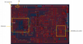
VDDA (pin 13) on the STM32L4333 for the DAC is filtered...

1755893812286.png


VSSA (pin 12) on the STM32L4333 for the DAC has a track to the battery negative pin (the same way its done on the Nucleo development board)...

1755894005216.png


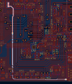
The DAC output track does run under the LED but I am suprised this causes interference....


1755894586060.png
 

Attachments

Last edited:

Rf300

Joined Apr 18, 2025
72
To be honest: Your layout is more than suboptimal, is is really bad. You routed your DAC-out-signal around all the other electronics including switching regulator on top of the PCB and your AGND-signal on the bottom. That creates a big loop, where any noise will be coupled into your analog signals.

You have to do a redesign of your PCB, change the placement of the CPU and the amplifier, so that the DAC-out is only a short route to the amplifier. If you haven't already used a 4-layer board, use it, with separae areas for DGND and AGND, connected only at that point, where your DAC-out signal is routed.

You have to reduce the loops, where signal and return current throug GND is flowing. GND-planes will help you.

EDIT: corrected typo
 
Last edited:

Thread Starter

freeflyer

Joined Sep 9, 2016
148
To be honest: Your layout is more than suboptimal, is is really bad. You routed your DAC-out-signal around all the other electronics including switching regulator on top of the PCB and your AGND-signal on the bottom. That creates a big loop, where any noise will be coupled into your analog signals.

You have to do a redesign of your PCB, change the placement of the CPU and the amplifier, so that the DAC-out is only a short route to the amplifier. If you haven't already used a 4-layer board, use it, with separae areas for DGND and AGND, connected only at that point, where your DAC-out signal is routed.

You have to reduce the loops, where signal and return current throug GND is flowing. GND-planes will help you.

EDIT: corrected typo
Thanks Rf300, not the news I wanted to hear but it is what it is.

On the NUCLEO-L433RC-P development board, VSSA (pin 12) for the DAC has a track to a header pin on the top layer...


1755954319369.png

And has a solder bridge (SB56) to main ground on the bottom layer....

1755954681720.png

1755954417701.png

What I find suprising is that the rats nest of wires and development boards (shown in the picture below) has less hiss and interference than my custom pcb !???

1755954982408.png

My PCB is a 4 layer board. Top and bottom layers are for signals and flooded with a ground plane.

Layer 2 is a GND plane...

1755955270348.png

Layer 3 is mainly 3.3V, with a copper pour shape for +5V and a few signal tracks...

1755955294829.png


Ideally I would have prefered to use an I2S audio amp, becuase a digital interface is less susceptible to noise than an analogue interface.

However, I am using a bluetooth audio receiver (MH-M18) which only has analouge outputs. Therefore I had to use an amplifier with an analogue interface, which also meant I had to use the DAC output of the ST MCU.

I mix the voice prompt audio (as heard in the video) with bluetooth audio. The bluetooth audio goes into IN1 on the LM48100Q amp.

I am not sure how to proceed, whether to search harder for an I2S solution or if I redesign the board exactly how to prevent this noise ? I dont want to spend another £200 for a pcb respin only to find the noise is still there.

I don't suppose there are any changes I can do to improve the issue on my current board ?
 
Last edited:

Rf300

Joined Apr 18, 2025
72
Maybe you can improve the behavior by connecting AGND to GND from C45/C46 directly to C43/C44 (if I read the reference designators correctly) by a very short piece of wire. So you can reduce the big AGND-loop from the battery input to the uC. This is the same functionality as SB56 on the Nucleo board.
 
Last edited:

Thread Starter

freeflyer

Joined Sep 9, 2016
148
Maybe you can improve the behavior by connecting AGND to GND from C45/C46 directly to C43/C44 (if I read the reference designators correctly) by a very short piece of wire. So you can reduce the big AGND-loop from the battery input to the uC. This is the same functionality as SB56 on the Nucleo board.
Thanks very much Rf300,

Can you confirm the diagram below is correct according to your suggestion please ?

Do I need also to cut the GNDA track on the bottom layer (blue) which goes back to the battery terminal, or just leave it connected ?

The redish area is a copper pour connected to GND, so I could just scratch some solder resist to connect the short wire from C45/C46 to GND ?

1755967544742.png


I have just been investigating futher and tried shorting IN2 of the amplifier to GND and this stopped this hissing...

1755967839897.png

I also tried a 1k and a 100k resistor to GND at the IN2 pin, it changed the hissing but did not reduce it. It also removed the bass (low frequency) from the audio.

The bluetooth audio, which is summed from stereo to mono at the amplifier IN1 input, does not appear to have the same hiss as the DAC audio. The left and right analogue tracks are routed similar to the DAC audio (but it only uses GND, there is no GNDA)...

1755968549596.png

1755968582832.png

Pin out of the MH-M18 bluetooth receiver...

1755968789616.png
 
Last edited:

Thread Starter

freeflyer

Joined Sep 9, 2016
148
I connected a short wire as shown in the picture below (I did not cut the GNDA track that goes back to the battery terminal) but the hiss still remains...

1755969647304.jpg
 

Thread Starter

freeflyer

Joined Sep 9, 2016
148
This does raise the question.... why does the bluetooth audio not have the same hiss that the DAC audio has, even though the tracks (left and right channel) are routed almost identically ?
 

Rf300

Joined Apr 18, 2025
72
How is your power supply scheme? Do you supply it by battery? How is the bluetooth module supplied? Where do the 3.3 V for the STM32 come from?
 

drjohsmith

Joined Dec 13, 2021
1,549
Layout is a hard process to learn, well done for trying,

You ask above as to why Bluetooth audio doe snot duffer the same as the analogue audio
Blue tooth is digital and digital is much less susceptible to noise that analogue

What your looking at is Electro Magnetic fields,

some good talks for free here
https://www.learnemc.com/emc-resources

The basics are "simple"

top of head:

The further apart the source of interference and the receiver are, the lower the interference

The higher impedance of the receiver, the more likely is interference from any given source

The bigger the source of interference, and the small the receiver voltages and currents are, the more likely one is going to suffer interference

The longer distance over which a source and receiver are close together, the greater the interference.

If a source and receiver need to be close, look at using a shield between and or use less susceptible signals like differential

A lot of noise is transmitted over power supplies

ground is a power supply !


Also be aware, the chip designers know their chip , and put layout help in the data sheet
https://www.ti.com/lit/ds/symlink/l...025430771&ref_url=https%3A%2F%2Fwww.ti.com%2F
 

Thread Starter

freeflyer

Joined Sep 9, 2016
148
Thanks drjohsmith

This is not the first PCB I have designed, I have designed PCBS on and off for the last 20 odd years and used 5+ different deisgn tools.

I have worked in automotive during that time as an electronis, embedded software and controls software engineer, mainly in R&D.

With regards to the bluetooth audio, I wish this was digital like you said. I designed the same project 10 years ago and used a WT32i bluetooth receiver that had I2S output. I used a CODEC to convert the I2S to analouge for a headphone amplifier and that design had no hiss or interference. Unfortunatley the WT32i is obsolete, plus it was too large for this redesign as I wanted to substantially shrink the size of the design.

Unofrtunatley the MH-18 bluetooth receiver (Jeli AC6925C) only has analouge outputs - on pin 6 (DACR) and pin 7 (DACL)....

1756028408964.png

So just like the STM32 DAC output, the bluetooth receiver interface is analogue. This is the reason I questioned why the interference is on the STM32 DAC but not the bluetooth DAC.

I followed the layout guidelines in the datasheet, as I always do. I even looked at the schematic, BOM and layout of the development boards too.

I used wide traces for the power supply and amplifier outputs, I placed bypass capacitors close to the device, I routed analouge traces along the edge of the board to keep them away from digital traces....

1756029249314.png

I wanted this board to work first time so spent a lot of time checking and modifying, even when PCB farbrication started. It took 3 respins of the PCB fabrication before they could start assembly. The second respin was due to a footprint error with the pressure sensor and third respin was due to a design change due to excessive current caused by the audio amplifier....

https://e2e.ti.com/support/audio-gr...he-i2cvdd-pin-when-the-vdd-pin-is-not-present

Originally I had the I2CVDD pin connected to +3.3V to match the I2C level of the STM32. However, the amplifer was drawing 25mA as current was leaking into the I2CVDD pin which actually powered the amplifier, even though the +5V on the VDD pin was disabled. So I had to change I2CVDD pin to be +5V and add a level shifter for the I2C data and clock lines.

1756029539440.png

My effort sort of paid off, as everything functions other than the noise on the audio and for some reason I am also seeing 2.5mA current draw when the MCU is shutdown, so this also needs investigating.

Since the issue I had with the amplifier I2CVDD pin, I am wondering if the amplifier is causing the 2.5mA current draw. I am also seeing 0.8V on the +5V supply when the +5V is disabled, so I am wondering if current is leaking through the 1k5 pull up resistor to +3.3V on the FAULT output of the amplifier (especially as 3.3/1k5 = 2.2mA).

I also wrote a post asking for help on the grounding of the STM32 DAC but responses were inconclusive...

https://forum.allaboutcircuits.com/...luetooth-receiver-and-audio-amplifier.207288/
 
Last edited:

Rf300

Joined Apr 18, 2025
72
Your power supply concept seems to be ok. You have to find the source of the hissing. In my opinion there are 2 possibilities.Either it is caused by coupling noise into the DAC-OUT signal or directly by the STM32.

Can you cut off the DAC-OUT signal on the PCB on both ends near the STM32 and the amplifier. Then connect the uC and the amplifier by a shielded audio cable or coax cable. It should be a few cm away from the PCB. Connect the shield at both ends to GND. If the hissing and the LED noise are reduced significantly then it is caused by coupling. Otherwise it is caused by the uC, then you have to think about better filtering of the uC supply.
 

Rf300

Joined Apr 18, 2025
72
I think, the 0.8 V at the + 5 V supply and therefore a part of the 2.5 mA is caused by "backwards feeding" of the amplifier via the pull-up R8 and the internal protection diodes of the FAULT-pin to + 5 V. I assume this is only a status signal to the uC, therefore you can increase the value to maybe 15 kOhm. This will not reduce the 0.8 V very much, but will reduce the 2.5 mA.
 

Thread Starter

freeflyer

Joined Sep 9, 2016
148
I think, the 0.8 V at the + 5 V supply and therefore a part of the 2.5 mA is caused by "backwards feeding" of the amplifier via the pull-up R8 and the internal protection diodes of the FAULT-pin to + 5 V. I assume this is only a status signal to the uC, therefore you can increase the value to maybe 15 kOhm. This will not reduce the 0.8 V very much, but will reduce the 2.5 mA.
Thanks Rf300, I removed the 1k5 resistor pull up on the FAULT line of the amp (I don’t currently use that signal anyway) and the current draw dropped to 1.5mA and the 5V rail is now 0V when the SMPS is disabled.

So an improvement, but still 1.5mA being drawn from something. With a 500mAh battery it will be discharged in a few weeks!
 

Thread Starter

freeflyer

Joined Sep 9, 2016
148
Your power supply concept seems to be ok. You have to find the source of the hissing. In my opinion there are 2 possibilities.Either it is caused by coupling noise into the DAC-OUT signal or directly by the STM32.

Can you cut off the DAC-OUT signal on the PCB on both ends near the STM32 and the amplifier. Then connect the uC and the amplifier by a shielded audio cable or coax cable. It should be a few cm away from the PCB. Connect the shield at both ends to GND. If the hissing and the LED noise are reduced significantly then it is caused by coupling. Otherwise it is caused by the uC, then you have to think about better filtering of the uC supply.
Thanks Rf300, is the fact that there is no hiss on the Bluetooth receiver DAC outputs which have very similar track routing a clue ?

I was going to ask if it’s worth trying shielded cable as you suggested. I can give it a go, but I think it will be tricky as it’s a small pcb using 0402 components. I could do with a microscope and tools to work on such a small pcb but only have a magnifying glass and standard soldering iron etc
 

drjohsmith

Joined Dec 13, 2021
1,549
the dac output of the sim is analog, can you look at the signal with a scope , see what the noise on that looks like ?

the the noise from turning on/ off the legs, did you get to bottom of that ?
 

Thread Starter

freeflyer

Joined Sep 9, 2016
148
the dac output of the sim is analog, can you look at the signal with a scope , see what the noise on that looks like ?

the the noise from turning on/ off the legs, did you get to bottom of that ?
I never found the cause of the hiss or interfence from the LED, I don't know where the source of the noise in coming from.

I will try the suggestion by Rf300 but it depends if I am able to solder shielded wire onto such a small board. I need to be careful not to damage it.

Ill get some scope traces of the bluetooth receiver DAC outputs (not sure what you mean by "sim is analog") ?
 

drjohsmith

Joined Dec 13, 2021
1,549
I never found the cause of the hiss or interfence from the LED, I don't know where the source of the noise in coming from.

I will try the suggestion by Rf300 but it depends if I am able to solder shielded wire onto such a small board. I need to be careful not to damage it.

Ill get some scope traces of the bluetooth receiver DAC outputs (not sure what you mean by "sim is analog") ?
what's the actual stm micro ?
does the micro have dedicated pins for power / ground / vref for the dac ?
if they have noise on them , that could be superimposed on the analog output of the stm dac.
 

Thread Starter

freeflyer

Joined Sep 9, 2016
148
what's the actual stm micro ?
does the micro have dedicated pins for power / ground / vref for the dac ?
if they have noise on them , that could be superimposed on the analog output of the stm dac.
Its an STM32L433

It does have dedicated pins (VDDA and VSSA) for all the analogue peripherals on the device.

I copied the development board (NUCLEO-L433RC-P) for pin VDDA and VSSA, there is a filter on the VDDA line.

The development board does not have hiss or interfence from the LED.

1756148737166.png

1756148852323.png

1756148875955.png
 

drjohsmith

Joined Dec 13, 2021
1,549
Its an STM32L433

It does have dedicated pins (VDDA and VSSA) for all the analogue peripherals on the device.

I copied the development board (NUCLEO-L433RC-P) for pin VDDA and VSSA, there is a filter on the VDDA line.

The development board does not have hiss or interfence from the LED.

View attachment 354779

View attachment 354781

View attachment 354782
Can I double check
The board you used as pattern , has by the looks of things a ferite bead, and then capacitor filtering to analog ground , with a very carefully placed connection between the analog and digital ground such that the led digital ground current does not flow through the analog ground .
On phone so difficult to read the layout , can you confirm you have done this analog ground / power split ?
 
Top