Am I doing SPI connections and stitching vias correctly?

Thread Starter

tdengineer

Joined Oct 21, 2025
36
spi stitching.png
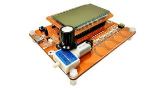
SPI trace length < 9mm

SPI Via size 0.3mm x 0.6mm

Stitching Ground Via Size 0.2mm x 0.4mm

I'm estimating .5ns or 500ps rise time

Frequency estimate 2-3 GHZ

I did the best I can I don't know if there is something I could be doing better.
I would like to reduce noise as much as possible.
very sensitive EEG signal electrode traces 10H distance away. 10H = 10x distance from spi trace to ground plane.
I heard Rick Hartley say 20H was necessary
 

lichurbagan

Joined Jul 4, 2025
120
Your SPI layout is generally well executed. Fast edges still create significant high-frequency noise. Add a tight ground via fence beside SPI. Place vias every one millimeter or less. This creates strong lateral electromagnetic shielding. Get more info about stitching vias here: https://www.pcbway.com/blog/PCB_Bas...re_Stitching_Vias_PCB_Knowledge_b1c5c187.html Add a ground guard trace around SPI pins. Tie the guard trace to the via fence. Keep the ground pour fully continuous. Avoid thin necks in ground areas. Add series resistors at SPI driver pins. Use 22–33 ohms for most signals. This slows edges and reduces EMI. Minimize parallel routing beside EEG traces. Move EEG traces inward if possible. Sandwich EEG between solid ground planes. Short SPI traces already help significantly. Maintain strict separation from analog domains. Ensure digital returns follow shortest paths. These steps greatly reduce EEG interference risk.
 

ronsimpson

Joined Oct 7, 2019
4,646
I would set the ground clearance to 1/2 of what you have. There are large holes in the ground.
1763218940287.png
Take DOUT left as far as you can while moving SCLK to the right, and CS left, etc. Maybe you could heal the broken grounds.
All the edges of the signals will return on the GND and VCC of IC left. Consider adding more GND VIAs on pin-33.
I don't see GND on IC-right. I think you want a good solid GND connection between the two ICs. (also VCC)
----edited----
You could reduce the size of the data VIAs to the size of the GND VIAs. That will close up the hole in the GND layer.
 
Last edited:

Thread Starter

tdengineer

Joined Oct 21, 2025
36
I would set the ground clearance to 1/2 of what you have. There are large holes in the ground.
View attachment 358912
Take DOUT left as far as you can while moving SCLK to the right, and CS left, etc. Maybe you could heal the broken grounds.
All the edges of the signals will return on the GND and VCC of IC left. Consider adding more GND VIAs on pin-33.
I don't see GND on IC-right. I think you want a good solid GND connection between the two ICs. (also VCC)
----edited----
You could reduce the size of the data VIAs to the size of the GND VIAs. That will close up the hole in the GND layer.
 

Attachments

Top