 Facebook
 Google
 GitHub
 Linkedin
I'm working on an FPGA-based fluence counter project (Z-turn Board V2 Xilinx XC7Z020) that requires designing an electronic board with three high-frequency input signals:
3.3V BNC TTL input.
5V BNC TTL input that is converted to 3.3V TTL using a level shifter.
NIM input at -0.8V that is converted to 3.3V TTL using a level shifter.
I need to protect the FPGA—specifically, the outputs from the level shifters (which are at 3.3V/0V)—using TVS protection diodes or others protection.
I need to protect my FPGA from Electrostatic Discharge (ESD). Given that these signals are high-frequency (in severeal Mhz like 10MHz) I know that I need a very low very low parasitic capacitance to avoid signal degradation.
Which TVS diodes (or integrated multi-diode circuits) or others components are best suited for this application? What key parameters (stand-off voltage, breakdown voltage, clamping voltage, capacitance) I should focus on for protecting these signals?
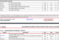
The maximum voltage of the FPGA pin input is here (Screenshot_1) : Zynq‐7000 SoC DC and AC Switching Characteristics
3.3V BNC TTL input.
5V BNC TTL input that is converted to 3.3V TTL using a level shifter.
NIM input at -0.8V that is converted to 3.3V TTL using a level shifter.
I need to protect the FPGA—specifically, the outputs from the level shifters (which are at 3.3V/0V)—using TVS protection diodes or others protection.
I need to protect my FPGA from Electrostatic Discharge (ESD). Given that these signals are high-frequency (in severeal Mhz like 10MHz) I know that I need a very low very low parasitic capacitance to avoid signal degradation.
Which TVS diodes (or integrated multi-diode circuits) or others components are best suited for this application? What key parameters (stand-off voltage, breakdown voltage, clamping voltage, capacitance) I should focus on for protecting these signals?
The maximum voltage of the FPGA pin input is here (Screenshot_1) : Zynq‐7000 SoC DC and AC Switching Characteristics
Attachments
-
 185.4 KB Views: 10


