Facebook
 Google
 GitHub
 Linkedin

ronsimpson
- Joined Oct 7, 2019
- 4,811
I agree with Irving. He has the right idea.
In my case, using GAN-MOSFETS I have to go beyond. You don't need to do what I say, this is just to show an example.
I get the next bigger caps for C1,C3 so I can get a wide trace out through the caps. (if needed)
I put the Gate driver on the right side, so the Gate-Out pin is "looking" right at the Gare of the MOSFET.
I try hard to not have VIAs in the Gate, and Gate return path. VIA adds a little inductance. (at 100khz it probably does not matter)
The loop of Gate-Driver to MOSFET and back to the IC needs to be small. A loop of wire makes an inductor. Try to make the diameter of the loop as small as you can.
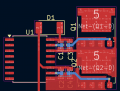
In my case, using GAN-MOSFETS I have to go beyond. You don't need to do what I say, this is just to show an example.
I get the next bigger caps for C1,C3 so I can get a wide trace out through the caps. (if needed)
I put the Gate driver on the right side, so the Gate-Out pin is "looking" right at the Gare of the MOSFET.
I try hard to not have VIAs in the Gate, and Gate return path. VIA adds a little inductance. (at 100khz it probably does not matter)
The loop of Gate-Driver to MOSFET and back to the IC needs to be small. A loop of wire makes an inductor. Try to make the diameter of the loop as small as you can.